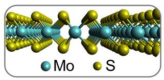
This schematic depicts the 2-D layer of MoS2 used in these experiments. As seen here, the layer is only three atoms thick, yet demonstrates amazing optical properties. Source: Christopher Petoukhoff
In the past decade, two-dimensional, 2D, materials have captured the fascination of a steadily increasing number of scientists. These materials, whose defining feature is having a thickness of only one to very few atoms, can be made of a variety of different elements or combinations thereof. Scientists’ enchantment with 2D materials began with Andre Geim and Konstantin Novoselov’s Nobel Prize winning experiment: creating a 2D material using a lump of graphite and common adhesive tape. This ingeniously simple experiment yielded an incredible material: graphene. This ultra-light material is roughly 200 times stronger than steel and is a superb conductor. Once scientists discovered that graphene had more impressive properties than its bulk component graphite, they decided to investigate other 2D materials to see if this was a universal property.
Christopher Petoukhoff, a Rutgers University graduate student working in the Femtosecond Spectroscopy Unit at the Okinawa Institute of Science and Technology Graduate University (OIST), studies a 2D material, made of molybdenum disulfide (MoS2). His research focuses on the 2D material’s optoelectronic applications, or how the material can detect and absorb light. Optoelectronics are ubiquitous in today’s world, from the photodetectors in automatic doors and hand dryers, to solar cells, to LED lights, but as anyone who has stood in front of an automatic sink desperately waving their hands around to get it to work will tell you, there is plenty of room for improvement. The 2D MoS2 is particularly interesting for use in photodetectors because of its capability of absorbing the same amount of light as 50nm of the currently used silicon-based technologies, while being 70 times thinner.
Petoukhoff, under the supervision of Professor Keshav Dani, seeks to improve optoelectronic devices by adding a 2D layer of MoS2 to an organic semiconductor, which has similar absorption strengths as MoS2. The theory behind using both materials is that the interaction between the MoS2 layer and the organic semiconductor should lead to efficient charge transfer. Petoukhoff’s research, published in ACS Nano, demonstrates for the first time that charge transfer between these two layers occurs at an ultra-fast timescale, on the order of less than 100 femtoseconds, or one tenth of one millionth of one millionth of a second.
The thinness of these materials, however, becomes a limiting factor in their efficiency as photovoltaics, or light-energy conversion devices. Light absorbing devices, such as solar cells and photodetectors, require a certain amount of optical thickness in order to absorb photons, rather than allowing them to pass through. To overcome this, researchers from the Femtosecond Spectroscopy Unit added an array of silver nanoparticles, or a plasmonic metasurface, to the organic semiconductor-MoS2 hybrid to focus and localize the light in the device. The addition of the metasurface increases the optical thickness of the material while capitalizing on the unique properties of the ultra-thin active layer, which ultimately increase the total absorption.
While this research is still in its infancy, its implications for the future are huge. Combinations with 2D materials have the potential to revolutionize the marketability of optoelectronic devices. Conventional optoelectronic devices are expensive to manufacture and are often made from scarce or toxic elements, such as indium or arsenic. Organic semiconductors have low manufacturing costs, and are made of earth-abundant and non-toxic elements. This research can potentially improve the cost and efficiency of optoelectronics, leading to better products in the future.


