Invigorating the idea of computers based on fluids instead of silicon, researchers at the National Institute of Standards and Technology (NIST) have shown how computational logic operations could be performed in a liquid medium by simulating the trapping of ions (charged atoms) in graphene (a sheet of carbon atoms) floating in saline solution. The scheme might also be used in applications such as water filtration, energy storage, or sensor technology.
The idea of using a liquid medium for computing has been around for decades, and various approaches have been proposed. Among its potential advantages, this approach would require very little material and its soft components could conform to custom shapes in, for example, the human body.
NIST’s ion-based transistor and logic operations are simpler in concept than earlier proposals. The new simulations show that a special film immersed in liquid can act like a solid silicon-based semiconductor. For example, the material can act like a transistor, the switch that carries out digital logic operations in a computer. The film can be switched on and off by tuning voltage levels like those induced by salt concentrations in biological systems.
“Previous devices were much more elaborate and complex,” NIST theorist Alex Smolyanitsky says. “What this ion-trapping approach achieves is conceptual simplicity. In addition, the same exact device can act as both a transistor and a memory device — all you have to do is switch the input and output. This is a feature that comes directly from ion trapping.”
The NIST molecular dynamics simulations focused on a graphene sheet 5.5 by 6.4 nanometers (nm) in size and with one or more small holes lined with oxygen atoms. These pores resemble crown ethers — electrically neutral circular molecules known to trap metal ions. Graphene is a sheet of carbon atoms arranged in hexagons, similar in shape to chicken wire, that conducts electricity and might be used to build circuits. This hexagonal design would seem to lend itself to pores, and in fact, other researchers have recently created crown-like holes in graphene in the laboratory.
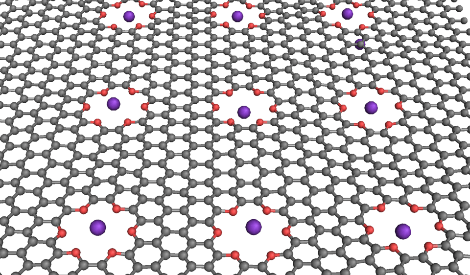
NIST researchers simulated computer logic operations in a saline solution with a graphene membrane (grey) containing oxygen-lined pores (red) that can trap potassium ions (purple) under certain electrical conditions. Image: NIST
In the NIST simulations, the graphene was suspended in water containing potassium chloride, a salt that splits into potassium and sodium ions. The crown ether pores were designed to trap potassium ions, which have a positive charge. Simulations show that trapping a single potassium ion in each pore prevents any penetration of additional loose ions through the graphene, and that trapping and penetration activity can be tuned by applying different voltage levels across the membrane, creating logic operations with 0s and 1s.
Ions trapped in the pores not only block additional ion penetration but also create an electrical barrier around the membrane. Just 1 nm away from the membrane, this electric field boosts the barrier, or energy needed for an ion to pass through, by 30 millivolts (mV) above that of the membrane itself.
Applying voltages of less than 150 mV across the membrane turns “off” any penetration. Essentially, at low voltages, the membrane is blocked by the trapped ions, while the process of loose ions knocking out the trapped ions is likely suppressed by the electrical barrier. Membrane penetration is switched on at voltages of 300 mV or more. As the voltage increases, the probability of losing trapped ions grows and knockout events become more common, encouraged by the weakening electrical barrier. In this way, the membrane acts like a semiconductor in transporting potassium ions.
To make actual devices, crown ether pores would need to be fabricated reliably in physical samples of graphene or other materials that are just a few atoms thick and conduct electricity. Other materials may offer attractive structures and functions. For example, transition metal dichalcogenides (a type of semiconductor) might be used because they are amenable to a range of pore structures and abilities to repel water.
The research is funded by the Materials Genome Initiative.
Source: NIST


