The measure by which any conductor is judged is how easily, and speedily, electrons can move through it. On this point, graphene is one of the most promising materials for a breathtaking array of applications. However, its ultra-high electron mobility is reduced when you synthesize larger sheets of the material. Now this barrier to industrial production of graphene may be broken as a result of new research done at KTH Royal Institute of Technology along with universities in Germany.
The long list of possible uses for graphene touches on nearly every dimension of future technologies, including those which address energy and health. Transistors, sensors, energy storage, flexible electronics, biomedicine and more can take advantage of its superior mechanical, electrical, thermal and optical properties. As a plus, it’s one atom thick and one of the strongest known materials ever measured.
But producing graphene on a large scale, while controlling and maintaining its unique properties, is a challenge yet to be realized. One of the main problems is the formation so-called “grain boundaries”, imperfections that appear in the material when synthesizing sheets of graphene (typically in the neighborhood of 100 mm × 100 mm or 150mm x 150mm) using a process known as chemical vapor deposition (CVD). The study, which was published in Science Advances, presents a simple, rapid and large-area observation of line defects in this wonder material.
The study’s lead author, Xuge Fan, who is doing his doctoral studies at KTH Royal Institute of Technology’s Department of Micro and Nanosystems, says that the boundaries are just what they sound like: tiny little seams in the two-dimensional honeycomb lattice pattern of graphene which scatter the flow of electrons and critically influence the graphene’s material properties.
“These are much like the seams of a patchwork quilt,” Fan says. “They are unavoidable, and for now we have to learn to live with them.”
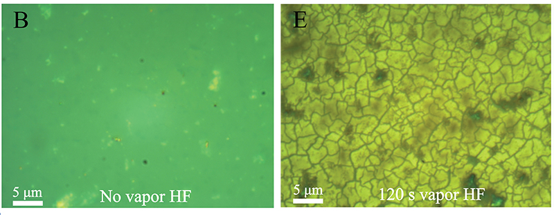
Image of graphene before and after VHF staining reveals (right) the grain boundaries of the material.
With proper visualization of graphene grain boundaries, scientists could make big gains in controlled engineering of these unavoidable defects. Fan says the study provides a method to simply, quickly and cost-effectively observe the size and distribution of grain boundaries on a large scale by using standard processes in wafer fabs, namely, vapor hydrofluoric acid (VHF) etching and optical microscope inspection.
“Up to now, no method exists that compares in simplicity, speed and scale to this methodology for visualizing grain boundaries in large-area CVD graphene on a silicon dioxide (SiO2) substrate,” he says.
Fan says that the method could be useful in speeding up the process of developing large-scale high quality graphene synthesis. “It offers a quick evaluation of the grain boundary density on large-area graphene samples, which takes no more than two minutes,” he says.
“It can also be used for post-mortem analysis of emerging graphene devices that use graphene patches — such as pressure sensors, transistors, and gas sensors — to study the effects of grain boundary line defects on device performance.”
The study was a collaboration between KTH, Rheinisch-Westfälische Technische Hochschule (RWTH), Aachen University, Chemnitz University of Technology, and the Gesellschaft für angewandte Mikro- und Optoelektronik mbH (AMO GmbH).
The research was funded by the European Research Council through the Starting Grants M&M’s (277879) and InteGraDe (307311), the Swedish Research Council (GEMS, 2015-05112), the China Scholarship Council (CSC), the German Federal Ministry for Education and Research (NanoGraM, BMBF, 03XP0006C),the German Research Foundation (DFG, LE 2440/1-2) and the German Research Council (DFG) through the Priority Program SPP 1459 Graphene.