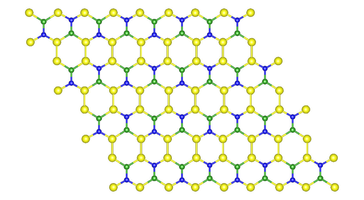
The 2D structure is a one-atom-thick flat material made up of silicon, boron and nitrogen—all light inexpensive and earth abundant elements—but most importantly—stable, something that other graphene alternatives lack. (Credit: Center for Computational Sciences, Univ. of Kentucky)
As scientists constantly seek to better graphene and advance digital technology—one physicist, along with two other colleagues, has developed a new material that just might be the answer to the commercial world’s current graphene problems.
Madhu Menon, Ph.D., associate director at the Center for Computational Sciences, University of Kentucky, in collaboration with scientists from Daimler in Germany and the Institute of Electronic Structure and Laser in Greece, worked on the ideal combination for a month by venturing beyond the first row of the periodic table and into the second row—taking silicon and seeing if it could merge with other elements in the first row—such as boron and nitrogen.
“No one really looked at what happens when you substitute some other carbon atom with silicon,” Menon told R&D Magazine. “I decided to go beyond the first row, where you have carbon, boron and nitrogen, and went to the second row where you have silicon and see if it can combine with other elements on the first floor.”
Menon experimented with a lot of different combinations that kept breaking up, but finally found one compilation that gave him a stable structure.
According to Physical Review B, Rapid Communications, the new material is a one atom-thick flat material made up of silicon, boron and nitrogen—all light inexpensive and earth abundant elements—but most importantly—stable, something that other graphene alternatives lack.
“One of the problems with graphene is that it’s all carbon. It’s metallic, so you cannot really use it in electronics, which requires a civic connector,” Menon added. “This new material has some advantages, it’s metallic as well but has silicon atoms in it, so it can attach to other items, such as hydrogen, so it makes it easier to integrate with existing silicon technology instead of making a drastic change with new material.”
Additionally, with graphene it’s not easy to put things on top for absorption, because carbon is already “happily bonded” to other carbons, so it doesn’t have any other bonding. But silicon is open to more bonding, according to the physicist.
The theoretical calculations were all performed virtually, via a computer by Menon, Ernst Richter from Daimler, who calculated the vibrations frequencies of the atoms and Antonis Andriotis from IESL, who helped with the stability analysis of the material.
Once the perfect combination was achieved, the next step was to test its stability. The team used the highest level of theory and simulations of heightened pressure conditions to see if the bonds would break or if the structure would disintegrate. They heated the material to 1,000-degree Celsius and it still did not break.
“The heat becomes the deciding factor in the stability of the device,” said Menon. “So all the tests indicate that this is a highly stable structure.”
According to the physicist, heat is basically the motion of the molecules, they vibrate. As the vibration increases, the temperature increases, so what you see on the computer is the vibrations of the atoms, telling you it’s heating up.
What’s most surprising about this discovery is that silicon is a bigger atom and doesn’t like to form 2D structures, but rather 3D structures, so it’s very unusual that silicon was able to be combined with boron and carbon nitrogen and still get a 2D structure.
“I’m making a drastic change with the new material,” Menon added.
The atoms in the new structure are arranged in a hexagonal pattern as in graphene, but that is where the similarity ends. The three elements that form the new material are all different sizes as are the bonds that connect the atoms. As a result, the sides of the hexagons formed by these atoms are unequal, unlike graphene.
While graphene is said to be the world’s strongest material with several unique properties, it has a downside—it isn’t a semiconductor and that’s why it doesn’t pan out in the digital technology industry. According to the study, subsequent search for new 2D semiconducting materials led researchers to a new class of three-layer materials called transition-metal dichalcogenides (TMDCs). These materials are mainly semiconductors that can be made into digital processors with greater efficiency than anything possible with silicon. But TMDCs are much bulkier than graphene and not made of earth abundant nor inexpensive materials.
Also, in addition to creating an electronic band gap, attachment of other elements can also be used to selectively change the band gap values—a key advantage over graphene.
This dilemma led Menon and his team to seek a lighter, more earth abundant and inexpensive material.
The theory is currently being worked into a material at a lab by the Mahendra Sunkara Conn Center for Renewable Energy Research at University of Louisville. This team has worked in close collaboration with Menon in the past. In fact, the project has recently received a $50,000 STIR grant from the U.S. Army. This money will partly be used to hire a Ph.D. student who could work full-time on this project, according to Menon.
The new 2D material discovery can be used for several applications, including electronics, armor, due to its light weight, and even solar energy.
“Any new material affords an opportunity to study a new science, virtually everything about it is unknown, so that presents an exciting opportunity to learn of lot of different physical properties,” Menon told R&D. “We can study how strong it is, how fast electrons can travel in it, what atoms attach to it, there are many, many things we can study here.”


