Research & Development World

  • Home Page
  • Topics
    • Aerospace
    • Archeology
    • Automotive
    • Biotech
    • Chemistry
    • Environment
    • Energy
    • Life Science
    • Material Science
    • R&D Market Pulse
    • R&D Management
    • Physics
  • Technology
    • 3D Printing
    • A.I./Robotics
    • Battery Technology
    • Imaging
    • Nanotechnology
    • Semiconductors
  • Controlled Environments
    • Cleanrooms
    • Graphene
    • Lasers
    • Regulations/Standards
    • Sensors
  • Scientific Computing
    • Big Data
    • HPC/Supercomputing
    • Informatics
    • Security
    • Software
  • R&D 100 Awards
    • ENTER NOW
    • 2020 Winners
    • Winner Archive
    • R&D 100 Conference
  • Resources
    • Digital Issues
    • Podcasts
    • Subscribe
  • 2021 Funding Forecast
  • COVID-19

Chemical Route Towards Electronic Devices in Graphene

By Aalto University | July 26, 2017

Schematic of the synthesis procedure for the graphene nanoribbon heterostructures: Precursor molecules are converted through chemical synthesis into precisely controlled graphene nanoribbons. Source: Image: Aalto University, Utrecht University, TU Delft

The 'wonder material' graphene has many interesting characteristics, and researchers around the world are looking for new ways to utilise them. Graphene itself does not have the characteristics needed to switch electrical currents on and off and smart solutions must be found for this particular problem. "We can make graphene structures with atomic precision. By selecting certain precursor substances (molecules), we can code the structure of the electrical circuit with extreme accuracy," explains Peter Liljeroth from Aalto University, who conceived the research project together with Ingmar Swart from Utrecht University.

Seamless integration

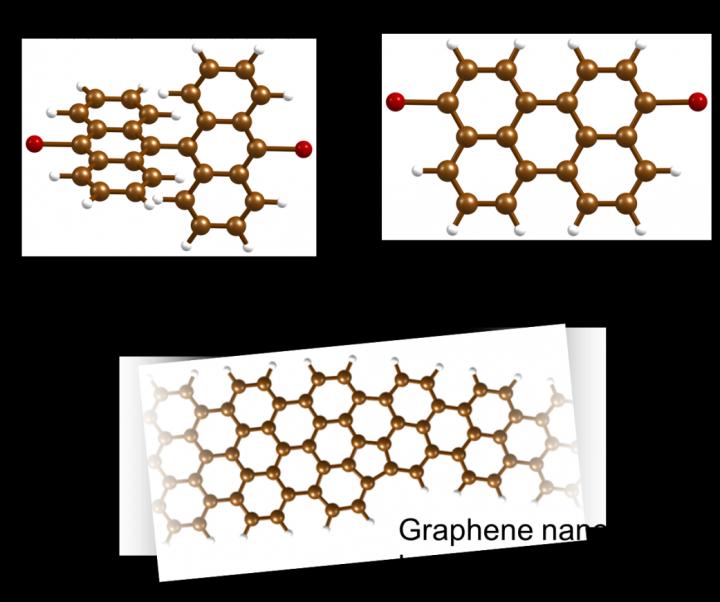
The electronic properties of graphene can be controlled by synthesizing it into very narrow strips (graphene nanoribbons). Previous research has shown that the ribbon's electronic characteristics are dependent on its atomic width. A ribbon that is five atoms wide behaves similarly to a metallic wire with extremely good conduction characteristics, but adding two atoms makes the ribbon a semiconductor. "We are now able to seamlessly integrate five atom-wide ribbons with seven atom-wide ribbons. That gives you a metal-semiconductor junction, which is a basic building block of electronic components," according to Ingmar Swart.

Chemistry on a surface

The researchers produced their electronic graphene structures through a chemical reaction. They evaporated the precursor molecules onto a gold crystal, where they react in a very controlled way to yield new chemical compounds. "This is a different method from that currently used to produce electrical nanostructures, such as those on computer chips. For graphene, it is so important that the structure is precise at the atomic level and it is likely that the chemical route is the only effective method," Ingmar Swart concludes.

Electronic characteristics

The researchers used advanced microscopic techniques to also determine the electronic and transport characteristics of the resulting structures. It was possible to measure electrical current through a graphene nanoribbon device with an exactly known atomic structure. "This is the first time where we can create e.g. a tunnel barrier and really know its exact atomic structure. Simultaneous measurement of electrical current through the device allows us to compare theory and experiment on a very quantitative level," says Peter Liljeroth.

Related Articles Read More >

With this new science, plastics could see a second life as biodegradable surfactants
Tires turned into graphene that makes stronger concrete
Wafer-thin nanopaper changes from firm to soft at the touch of a button
Airplanes to cellphones: New equipment finds the flaws in everything

Need R&D World news in a minute?

We Deliver!
R&D World Enewsletters get you caught up on all the mission critical news you need in research and development. Sign up today.
Enews Signup
Tweets by @RandDWorld

R&D World Digital Issues

February 2020 issue

Browse the most current issue of R&D World and back issues in an easy to use high quality format. Clip, share and download with the leading R& magazine today.

Research & Development World
  • Subscribe to R&D World Magazine
  • Enews Sign Up
  • Contact Us
  • Drug Discovery & Development
  • Pharmaceutical Processing
  • 2021 Global Funding Forecast

Copyright © 2021 WTWH Media LLC. All Rights Reserved. The material on this site may not be reproduced, distributed, transmitted, cached or otherwise used, except with the prior written permission of WTWH Media
Privacy Policy | Advertising | About Us

Search R&D World

  • Home Page
  • Topics
    • Aerospace
    • Archeology
    • Automotive
    • Biotech
    • Chemistry
    • Environment
    • Energy
    • Life Science
    • Material Science
    • R&D Market Pulse
    • R&D Management
    • Physics
  • Technology
    • 3D Printing
    • A.I./Robotics
    • Battery Technology
    • Imaging
    • Nanotechnology
    • Semiconductors
  • Controlled Environments
    • Cleanrooms
    • Graphene
    • Lasers
    • Regulations/Standards
    • Sensors
  • Scientific Computing
    • Big Data
    • HPC/Supercomputing
    • Informatics
    • Security
    • Software
  • R&D 100 Awards
    • ENTER NOW
    • 2020 Winners
    • Winner Archive
    • R&D 100 Conference
  • Resources
    • Digital Issues
    • Podcasts
    • Subscribe
  • 2021 Funding Forecast
  • COVID-19