Research & Development World

  • R&D World Home
  • Topics
    • Aerospace
    • Automotive
    • Biotech
    • Careers
    • Chemistry
    • Environment
    • Energy
    • Life Science
    • Material Science
    • R&D Management
    • Physics
  • Technology
    • 3D Printing
    • A.I./Robotics
    • Software
    • Battery Technology
    • Controlled Environments
      • Cleanrooms
      • Graphene
      • Lasers
      • Regulations/Standards
      • Sensors
    • Imaging
    • Nanotechnology
    • Scientific Computing
      • Big Data
      • HPC/Supercomputing
      • Informatics
      • Security
    • Semiconductors
  • R&D Market Pulse
  • R&D 100
    • Call for Nominations: The 2025 R&D 100 Awards
    • R&D 100 Awards Event
    • R&D 100 Submissions
    • Winner Archive
    • Explore the 2024 R&D 100 award winners and finalists
  • Resources
    • Research Reports
    • Digital Issues
    • R&D Index
    • Subscribe
    • Video
    • Webinars
  • Global Funding Forecast
  • Top Labs
  • Advertise
  • SUBSCRIBE

Converting Crystals into Erasable Electronics

By Kenny Walter | July 27, 2017

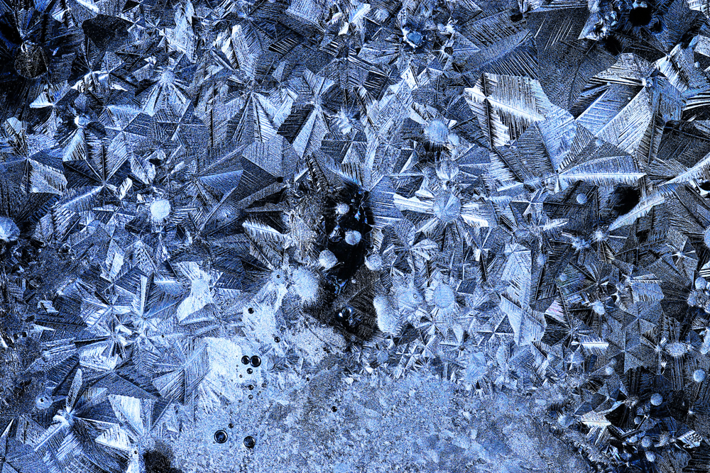
New research has found that a crystal can be converted into an electrical circuit, paving the way for a bevy of new electronic devices.

Researchers at Washington State University have developed a method to write an electrical circuit into a crystal, which could result in transparent, 3D electronics that can be erased and reconfigured, similar to an Etch A Sketch.

The research team used a laser to etch a line in the crystal that carried a current, with electrical contacts at each end of the line.

“It opens up a new type of electronics where you can define a circuit optically and then erase it and define a new one,” Matt McCluskey, a WSU professor of physics and materials science, said in a statement. “It’s exciting that it’s reconfigurable.

“It’s also transparent. There are certain applications where it would be neat to have a circuit that is on a window or something like that, where it actually is invisible electronics,” he added.

Crystals do not usually conduct electricity, but when the crystal strontium titanate is heated under the right conditions, it can be altered so light will make it conductive.

Persistent photoconductivity—a phenomenon where materials become much more conductive when light is shone on them—also occurs at room temperature, an improvement over materials that require cooling with liquid nitrogen.

“We’re still trying to figure out exactly what happens,” McCluskey said, adding that heat forces strontium atoms to leave the material, creating light-sensitive defects responsible for the persistent photoconductivity.

The work builds on previously research from 2013, when a doctoral student discovered a 400-fold increase in the electrical conductivity of a crystal by leaving it exposed to light.

In the new research, McCluskey was able to increase the crystal’s conductivity 1,000-fold for up to a year with the ability to be erased by heating it on a hot plate and recast with an optical pen.

“We look at samples that we exposed to light a year ago and they’re still conducting,” he said. “It may not retain 100 percent of its conductivity, but it’s pretty big.

“It’s an Etch A Sketch,” he added. “We’ve done it a few cycles. Another engineering challenge would be to do that thousands of times.”

  The study was published in Scientific Reports.

Related Articles Read More >

KIST carbon nanotube supercapacitor holds capacity after 100,000 cycles
A new wave of metalworking lets semiconductor crystals bend and stretch
LLNL deposits quantum dots on corrugated IR chips in a single step
KATRIN inauguration photo form 2018
Neutrinos pinned below 0.45 eV; KATRIN halves the particle’s mass ceiling
rd newsletter
EXPAND YOUR KNOWLEDGE AND STAY CONNECTED
Get the latest info on technologies, trends, and strategies in Research & Development.
RD 25 Power Index

R&D World Digital Issues

Fall 2024 issue

Browse the most current issue of R&D World and back issues in an easy to use high quality format. Clip, share and download with the leading R&D magazine today.

Research & Development World
  • Subscribe to R&D World Magazine
  • Enews Sign Up
  • Contact Us
  • About Us
  • Drug Discovery & Development
  • Pharmaceutical Processing
  • Global Funding Forecast

Copyright © 2025 WTWH Media LLC. All Rights Reserved. The material on this site may not be reproduced, distributed, transmitted, cached or otherwise used, except with the prior written permission of WTWH Media
Privacy Policy | Advertising | About Us

Search R&D World

  • R&D World Home
  • Topics
    • Aerospace
    • Automotive
    • Biotech
    • Careers
    • Chemistry
    • Environment
    • Energy
    • Life Science
    • Material Science
    • R&D Management
    • Physics
  • Technology
    • 3D Printing
    • A.I./Robotics
    • Software
    • Battery Technology
    • Controlled Environments
      • Cleanrooms
      • Graphene
      • Lasers
      • Regulations/Standards
      • Sensors
    • Imaging
    • Nanotechnology
    • Scientific Computing
      • Big Data
      • HPC/Supercomputing
      • Informatics
      • Security
    • Semiconductors
  • R&D Market Pulse
  • R&D 100
    • Call for Nominations: The 2025 R&D 100 Awards
    • R&D 100 Awards Event
    • R&D 100 Submissions
    • Winner Archive
    • Explore the 2024 R&D 100 award winners and finalists
  • Resources
    • Research Reports
    • Digital Issues
    • R&D Index
    • Subscribe
    • Video
    • Webinars
  • Global Funding Forecast
  • Top Labs
  • Advertise
  • SUBSCRIBE