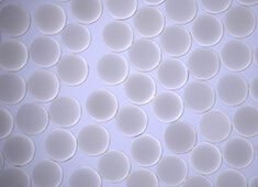
While diamonds may be a girl’s best friend, they’re also well loved by scientists working to enhance the performance of electronic devices. Two new studies performed at Argonne have revealed a new pathway for materials scientists to use previously unexplored properties of nanocrystalline-diamond thin films. Image: Argonne National Laboratory |
While
diamonds may be a girl’s best friend, they’re also well loved by scientists
working to enhance the performance of electronic devices.
Two new
studies performed at the United States Department of Energy’s Argonne National
Laboratory have revealed a new pathway for materials scientists to use
previously unexplored properties of nanocrystalline-diamond thin films. While
the properties of diamond thin films are relatively well understood, the new
discovery could dramatically improve the performance of certain types of
integrated circuits by reducing their “thermal budget.”
For
decades, engineers have sought to build more efficient electronic devices by
reducing the size of their components. In the process of doing so, however,
researchers have reached a “thermal bottleneck,” said Argonne nanoscientist Anirudha Sumant.
In a
thermal bottleneck, the excess heat generated in the device causes undesirable
effects that affect its performance. “Unless we come-up with innovative
ways to suck the heat off of our electronics, we are pretty much stuck with
this bottleneck,” Sumant explained.
The
unusually attractive thermal properties of diamond thin films have led
scientists to suggest using this material as a heat sink that could be
integrated with a number of different semiconducting materials. However, the
deposition temperatures for the diamond films typically exceed 800 C—roughly 1,500
F, which limits the feasibility of this approach.
“The
name of the game is to produce diamond films at the lowest possible
temperature. If I can grow the films at 400 C, it makes it possible for me to
integrate this material with a whole range of other semiconductor
materials,” Sumant said.
By using a
new technique that altered the deposition process of the diamond films, Sumant
and his colleagues at Argonne’s Center for
Nanoscale Materials were able to both reduce the temperature to close to 400 C
and to tune the thermal properties of the diamond films by controlling their
grain size. This permitted the eventual combination of the diamond with two
other important materials: graphene and gallium nitride.
According
to Sumant, diamond has much better heat conduction properties than silicon or
silicon oxide, which were traditionally used for fabrication of graphene
devices. As a result of better heat removal, graphene devices fabricated on
diamond can sustain much higher current densities.
In the
other study, Sumant used the same technology to combine diamond thin films with
gallium nitride, which is used extensively in high-power light-emitting devices
(LED). After depositing a 300-nm-thick diamond film on a gallium nitride
substrate, Sumant and his colleagues noticed a considerable improvement in the
thermal performance. Because a difference within an integrated circuit of just
a few degrees can cause a noticeable change in performance, he called this
result “remarkable.”
“The
common link between these experiments is that we’re finding new ways of
dissipating heat more effectively while using less energy, which is the
key,” Sumant said. “These processes are crucial for industry as they
look for ways to overcome conventional limits on semiconducting circuits and
pursue the next generation of electronics.”
The
results of the two studies were reported in Nano
Letters and Advanced Functional
Materials.


