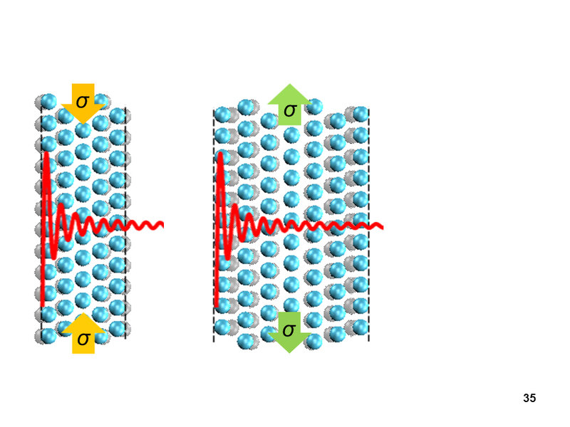
Quantum mechanics, literally: the schematic diagram illustrates how a mechanical stress develops in aluminium nanofilms of five and seven atomic layers thick due to quantum effects. The electron energy, represented in the decaying oscillation, depends on the film thickness. To reach an electron energy minimum, the film thickness must change. A film of five atomic layers thick is forced to compress perpendicular to the surface, where in contrast, a seven-atomic layer film relaxes perpendicular to the surface. Parallel to the film the system wants to simultaneously expand or contract, respectively. However, this is impossible because the aluminium atoms are fixed on the substrate. Therefore a compressive or tensile stress develops that is shown by the yellow arrows. They signify the force that develops to prevent the respective expansion or contraction. David Flötotto / MPI for Intelligent Systems |

Read
heads in hard drives, lasers in DVD players, transistors on computer
chips, and many other components all contain ultrathin films of metal or
semiconductor materials. Stresses arise in thin films during their
manufacture. These influence the optical and magnetic properties of the
components, but also cause defects in crystal lattices, and in the end,
lead to component failure.
As
researchers in the department of Eric Mittemeijer at the Max Planck
Institute for Intelligent Systems in Stuttgart have now established,
enormous stresses in the films are created by a quantum-mechanical
mechanism that has been unknown until now, based on an effect by the
name of quantum confinement. This effect can cause stresses equivalent
to one thousand times standard atmospheric pressure, dependent of
thickness. Knowledge of this could be helpful in controlling the optical
and mechanical properties of thin-film systems and increase their
mechanical stability. Additionally, very sensitive sensors might also be
developed on the basis of this knowledge.
Films
of metal, semiconductor materials or ceramics can be grown today one
atomic layer at a time onto crystalline substrates such as silicon.
Despite this atomic precision, defects invariably arise in crystal
lattices of films only a few nanometres thick; sometimes only one atom
is missing in a lattice where one should actually be. These kinds of
lattice defects can impair the efficiency of solar cells or
semiconductor lasers. One reason for this are stresses that arise in the
film. Up to now, the main reason for these stresses was considered to
be the growth of the film on a different material, so that the crystal
lattice of the film did not coincide with that of the substrate. The
atomic separations in the film were correspondingly contracted or
expanded, with a compressive or tensile stress developing. Materials
scientists working with Eric Mittemeijer, Director at the Max Planck
Institute for Intelligent Systems in Stuttgart, have now discovered an
additional mechanism that is able to create enormous stress in the
ultrathin films.
David
Flötotto and his colleagues discovered this mechanism as they analysed
the stress in ultrathin aluminium films. They used an apparatus for this
that precisely lays down one layer after another of aluminium atoms
onto a silicon substrate, just the way a brick wall is built. By first
measuring the stress in one single layer, then in a double-layer, a
triple-layer and so on, the researchers found out how the stress in the
aluminium film changed after deposition of each new layer. To do this,
they determined how much the silicon substrate deformed due to this
stress. And in doing so, they surprisingly established that the stress
in the film fluctuated by about 100 megapascals as it thickened. By
comparison, the standard pressure of the atmosphere at sea level amounts
to about 0.1 megapascal.
The film expands and contracts, seeking the energy minimum
The
foundation for this phenomenon lies in the electrons behaving
differently in a thin film of a few atomic layers than in a thicker
film. Due to quantum mechanics, the elementary particles are described
not just as particles, but as waves as well. Since the thickness of
films a few atomic layers thick is only somewhat larger than the
wavelength of electrons, the electrons “sense” the boundaries of the
film. This so-called quantum confinement sharply reduces the flexibility
of electrons in absorbing and releasing energy. The electrons therefore
only occupy discrete energy states.
The
electron energy fluctuates with the continuously increasing film
thickness. It first increases with thickness, then decreases, increases
again, and so on. The principle that applies here is that everything
possible will be done to minimize the energy of the system. The film
seeks thicknesses for which the electron energy is as small as possible,
i.e. the minima of this fluctuation. If the film grows one new atom
layer thicker, it is either a bit too thick or too thin for this
minimum. In the first case, it contracts, in the latter case it expands
in order to attain the minimum energy.
The properties of ultrathin films can now be more suitably tailored
Expansion
or contraction of the film thickness results in the atomic lattice
parallel to the film wanting to expand or contract, respectively.
Because it cannot do that due to its fixed connection to the substrate, a
tensile or compressive stress develops in the film that the researchers
have measured. When the film thickness has been augmented to five
atomic layers, it contracts, and at seven atomic layers, it expands. To
explain the stresses measured, the researchers in Stuttgart developed a
model combining the theory of free electrons and Hooke’s Law, as it is
known, which describes the elastic behaviour of solid bodies.
The
researchers see many potential applications for their discovery. “The
better one understands how stresses develop in a thickening film, the
better one can control its growth and avoid lattice defects,” says David
Flötotto. Moreover, the mechanical strain in a thin film influences its
electrical, optical and magnetic properties.
“Properties
such as these can now be tailored better for ultrathin films,” Flötotto
is convinced. The measurements of the stress can also be used to
determine the thickness of a growing film very precisely. One could also
exploit the effect not least for highly sensitive gas sensors. Because
upon deposition of even the smallest amounts of gas onto the surface,
the energy state of the electrons and thus the stresses in the film are
altered.
The
team is now working on making the effect viable for thick films as well
(in the range of 100 nanometres). “We are working at the moment on
freezing the state of the stress in order to control stress in a thicker
film as well,” says Flötotto. Properties like its mechanical stability
can thus be improved.
Source: Max Planck Institute


