Research & Development World

  • Home Page
  • Topics
    • Aerospace
    • Archeology
    • Automotive
    • Biotech
    • Chemistry
    • COVID-19
    • Environment
    • Energy
    • Life Science
    • Material Science
    • R&D Market Pulse
    • R&D Management
    • Physics
  • Technology
    • 3D Printing
    • A.I./Robotics
    • Battery Technology
    • Controlled Environments
      • Cleanrooms
      • Graphene
      • Lasers
      • Regulations/Standards
      • Sensors
    • Imaging
    • Nanotechnology
    • Scientific Computing
      • Big Data
      • HPC/Supercomputing
      • Informatics
      • Security
      • Software
    • Semiconductors
  • 2021 R&D 100 Award Winners
    • R&D 100 Awards
    • 2020 Winners
    • Winner Archive
  • Resources
    • Digital Issues
    • Podcasts
    • Subscribe
  • Global Funding Forecast
  • Webinars

Doped-Up Semiconductors Lead to Next-Gen Electronics

By Aalto University | November 10, 2017

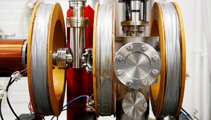
Sample chamber of the positron accelerator. Image: Hanna Koikkalainen

Physicists at Aalto University have made a breakthrough in revising methods largely discarded 15 years ago. They have discovered a microscopic mechanism that will allow gallium nitride semiconductors to be used in electronic devices that distribute large amounts of electric power.

The trick is to be able to use beryllium atoms in gallium nitride. Gallium nitride is a compound widely used in semiconductors in consumer electronics from LED lights to game consoles. To be useful in devices that need to process considerably more energy than in your everyday home entertainment, though, gallium nitride needs to be manipulated in new ways on the atomic level.

“There is growing demand for semiconducting gallium nitride in the power electronics industry. To make electronic devices that can process the amounts of power required in, say, electric cars, we need structures based on large-area semi-insulating semiconductors with properties that allow minimizing power loss and can dissipate heat efficiently. To achieve this, adding beryllium into gallium nitride — or ‘doping’ it — shows great promise,” explains Professor Filip Tuomisto from Aalto University.

Experiments with beryllium doping were conducted in the late 1990s in the hope that beryllium would prove more efficient as a doping agent than the prevailing magnesium used in LED lights. The work proved unsuccessful, however, and research on beryllium was largely discarded.

Working with scientists in Texas and Warsaw, researchers at Aalto University have now managed to show — thanks to advances in computer modelling and experimental techniques — that beryllium can actually perform useful functions in gallium nitride. The article published in Physical Review Letters shows that depending on whether the material is heated or cooled, beryllium atoms will switch positions, changing their nature of either donating or accepting electrons.

“Our results provide valuable knowledge for experimental scientists about the fundamentals of how beryllium changes its behavior during the manufacturing process. During it — while being subjected to high temperatures — the doped compound functions very differently than the end result,” describes Tuomisto.

If the beryllium-doped gallium nitride structures and their electronic properties can be fully controlled, power electronics could move to a whole new realm of energy efficiency.

“The magnitude of the change in energy efficiency could as be similar as when we moved to LED lights from traditional incandescent light bulbs. It could be possible to cut down the global power consumption by up to ten percent by cutting the energy losses in power distribution systems,” says Tuomisto.

Source: Aalto University

Related Articles Read More >

‘Self-driving’ lab speeds up research, synthesis of energy materials
Record-breaking, ultrafast devices step to protecting the grid from EMPs
Surprising semiconductor properties revealed with innovative new method
Thermo Scientific Centrios HX offers precise circuit edit solution for fast prototyping
2021 R&D Global Funding Forecast

Need R&D World news in a minute?

We Deliver!
R&D World Enewsletters get you caught up on all the mission critical news you need in research and development. Sign up today.
Enews Signup

R&D World Digital Issues

February 2020 issue

Browse the most current issue of R&D World and back issues in an easy to use high quality format. Clip, share and download with the leading R& magazine today.

Research & Development World
  • Subscribe to R&D World Magazine
  • Enews Sign Up
  • Contact Us
  • About Us
  • Drug Discovery & Development
  • Pharmaceutical Processing
  • 2022 Global Funding Forecast

Copyright © 2022 WTWH Media LLC. All Rights Reserved. The material on this site may not be reproduced, distributed, transmitted, cached or otherwise used, except with the prior written permission of WTWH Media
Privacy Policy | Advertising | About Us

Search R&D World

  • Home Page
  • Topics
    • Aerospace
    • Archeology
    • Automotive
    • Biotech
    • Chemistry
    • COVID-19
    • Environment
    • Energy
    • Life Science
    • Material Science
    • R&D Market Pulse
    • R&D Management
    • Physics
  • Technology
    • 3D Printing
    • A.I./Robotics
    • Battery Technology
    • Controlled Environments
      • Cleanrooms
      • Graphene
      • Lasers
      • Regulations/Standards
      • Sensors
    • Imaging
    • Nanotechnology
    • Scientific Computing
      • Big Data
      • HPC/Supercomputing
      • Informatics
      • Security
      • Software
    • Semiconductors
  • 2021 R&D 100 Award Winners
    • R&D 100 Awards
    • 2020 Winners
    • Winner Archive
  • Resources
    • Digital Issues
    • Podcasts
    • Subscribe
  • Global Funding Forecast
  • Webinars