 Physicists at Forschungszentrum Jülich have discovered unexpected effects in doped graphene — i.e. graphene that is mixed with foreign atoms. They investigated samples of the carbon compound enriched with the foreign atom nitrogen on various substrate materials. Unwanted interactions with these substrates can influence the electric properties of graphene. The researchers at the Peter Grünberg Institute have now shown that effective doping depends on the choice of substrate material. The scientists’ results were published in the journal Physical Review Letters.
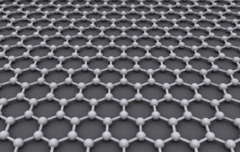
Harder than diamond and tougher than steel, light weight, transparent, flexible, and extremely conductive: the mesh material graphene is regarded as the material of the future. It could make computers faster, mobile phones more flexible, and touchscreens thinner. But so far, the industrial production of the carbon lattice, which is only one atom thick, has proven problematic: in almost all cases, a substrate is required. The search for a suitable material for this purpose is one of the major challenges on the path towards practical applications because if undesirable interactions occur, they can cause the graphene to lose its electric properties.
For some years, scientists have been testing silicon carbide — a crystalline compound of silicon and carbon — for its suitability as a substrate material. When the material is heated to more than 1400 degrees Celsius in an argon atmosphere, graphene can be grown on the crystal. However, this “epitaxial monolayer graphene” displays — very slight — interaction with the substrate, which limits its electron mobility.
In order to circumvent this problem, hydrogen is introduced into the interface between the two materials. This method is known as hydrogen intercalation. The bonds between the graphene and the substrate material are separated and saturated by the hydrogen atoms. This suppresses the electronic influence of the silicon crystal while the graphene stays mechanically joined with the substrate: quasi-free-standing monolayer graphene.
For practical applications, the electrical properties of graphene must be modifiable — for example by introducing additional electrons into the material. This is effected by targeted “contamination” of the carbon lattice with foreign atoms. For this process, known as doping, the graphene is bombarded with nitrogen ions and then annealed. This results in defects in the lattice structure: some few carbon atoms — fewer than 1 percent — separate from the lattice and are replaced with nitrogen atoms, which bring along additional electrons.
Scientists at Jülich’s Peter Grünberg Institute — Functional Nanostructures at Surfaces (PGI-3) have now, for the first time, studied whether and how the structure of the substrate material influences this doping process. At the synchrotron radiation source Diamond Light Source in Didcot, U.K., François C. Bocquet and his colleagues doped samples of epitaxial and quasi-free-standing monolayer graphene and investigated its structural and electronic properties. By means of standing X-ray wave fields, they were able to scan both graphene and substrate at a precision of a few millionths of a micrometer — less than a tenth of the radius of an atom.
Their findings were surprising. “Some of the nitrogen atoms diffused from the graphene into the silicon carbide,” explains Bocquet. “It was previously believed that the nitrogen bombardment only affected the graphene, but not the substrate material.”
Although both samples were treated in the same way, they exhibited different nitrogen concentrations, but almost identical electronic doping: not all nitrogen atoms were integrated in the graphene lattice, nevertheless the number of electrons in the graphene rose as if this were the case. The key to this unexpected result lies in the different behavior of the interface layers between graphene and substrate. For the epitaxial graphene, nothing changed: the interface layer remained stable, the structure unchanged. In the quasi-free-standing graphene, however, some of the hydrogen atoms between graphene and substrate were replaced with nitrogen atoms. According to Bocquet: “If you examine the quasi-free-standing graphene, you will find a nitrogen atom underneath the graphene coat in some places. These nitrogen atoms, although they are not part of the graphene, can dope the lattice without destroying it. This unforeseen result is very promising for future applications in micro- and nanoelectronics.”
Source: Forschungszentrum Jülich


