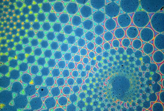
The stop-flow photopatterning method allows for intricate polymer brush patterns. Source: Christian Pester
Antimicrobial cutting boards. Flame-retardant carpets. Friction-resistant bearings. Engineered surfaces add value to the things we use, providing extra layers of safety, easing their operation, preserving their quality or adding utility.
At UC Santa Barbara, materials researchers are looking to greatly improve on the concept with a method of micron-scale surface chemical patterning that can not only decrease time and money spent in their manufacture, but also add versatility to their design. In a paper describing a method called “sequential stop-flow photopatterning,” UCSB materials scientists describe a new platform for functionalizing and engineering surfaces with patterned polymer brushes.
“It’s a really powerful tool you can use for many purposes,” said Christian Pester, a postdoctoral researcher in the Craig Hawker Lab at UCSB. He is the lead author of the paper, which appears in the journal Advanced Materials.
If you take a close look at some engineered surfaces, you’ll see that at the micro- and nanoscale, they aren’t flat and empty, but rather consist of infinitesimal elongated polymer molecules attached at one end to the surface. These polymer brushes imbue the surface with various properties and functions. They can, for instance, repel water, prevent bacteria from attaching, enhance drug delivery or attract other molecules. Patterning polymer brushes allows the combination of multiple functionalities.
Conventional methods of patterning polymer brushes on surfaces are often repetitive and time-consuming, Pester said. For more than one brush, the first polymer growth from an initiating “seed” must be deactivated and the synthetic process repeated after re-depositing new initiating molecules. It can take up to the better part of a day for each type of polymer brush, he added.
With sequential stop-flow photopatterning, the intermediate steps can be eliminated, Pester said.
“It’s also chemically more clean, because you’re not iteratively depositing the initiator,” he said, “which means you’re also taking away related washing and cleansing steps.”
To accomplish this feat, the substrate (with initiating molecules deposited) is enclosed in a stop-flow cell and a solution streamed in. Irradiation with light can then initiate the reaction. A separate photomask — essentially a sort of stencil — is positioned over the top of the cell, thus allowing only some light-activated growth. After the growth step, the light is turned off, the first solution is drained from the cell and a second one is flowed in to functionalize the polymers. Since neither the mask nor the substrate has been moved, only the molecules that have been exposed to light are grown and functionalized. These basic steps may be repeated with variations in the reactants, the light source or the positions of the substrate or the photomask to create polymer brush patterns in a single continuous process.
“We can also create chemical and height gradients on the nanoscale,” Pester said, features that are only indirectly accessible with conventional methods.
The technology opens the door to increased versatility in the development of polymer brushes with an eye toward industrial applications. Pester credits the collaborative nature of UCSB research for this scientific development, which is dedicated to the late Edward J. Kramer, materials professor and founder of the campus’s Materials Research Laboratory. “I think what is really cool about this project and I think where UCSB shines is in collaboration,” said Pester.


