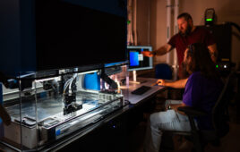
Traps. Whether you’re squaring off against the Empire or trying to wring electricity out of sunlight, they’re almost never a good thing. But sometimes you can turn that trap to your advantage. A team from the Univ. of Nebraska-Lincoln, working with researchers at NIST, has shown that electron-trapping defects that are typically problematic in solar cells can be an asset when engineering sensitive light detectors.
Their work, which appear in Advanced Materials, suggests that these defects could be harnessed to make light sensors that consume very low power and could be used for imaging, spectroscopy and other industrial and scientific applications.
For the past few years, researchers have been studying films of organometal trihalide perovskites—OTPs for short—for use in solar cells, because they have several attractive qualities.
For one, they are relatively easy to make. A solution of the material is poured over a fast-spinning disk. The spinning disk throws off excess and the solution—now much thinner than a typical coat of paint—is dried. Even though the films are only a few hundred nanometers thick, they can still absorb most of the light that hits them.
So far, competing materials that also are “solution-processable” have been hindered by their relative inability to conduct light-generated electrical charges, a property known as carrier mobility. But OTPs’ carrier mobility is comparable to that of crystalline silicon. Potentially, it could be a gamechanger that would allow the engineering of high-performance, light-harnessing devices at low cost.
When a photon is absorbed by a light-sensitive material, it transfers energy to a negatively charged electron, which goes to an excited state and leaves behind an empty spot, called a hole, which is positively charged. To make use of the absorbed energy in a solar cell or light detector, these oppositely charged carriers must drift in opposite directions towards different electrodes. Material defects that “trap” either the electrons or the holes reduce carrier mobility and degrade the device’s performance.
The research team led by the Univ. of Nebraska-Lincoln found that although trap states in the bulk material are bad for solar cells, surface defects and traps close to the electrodes in OTPs can be engineered to boost their light-detecting performance.
“To detect light, one measures changes that occur in a material when a photon hits it,” says NIST’s Andrea Centrone. “One way to increase a detector’s sensitivity to light is to apply a voltage to it. Traps located near the electrodes lower the energy barrier for injecting electrons into the material. In our devices, lowering the barrier effectively multiplies the material’s light sensitivity up to 500 times when we apply the right voltage.”
Centrone explains that trap states only have this multiplying effect if they are located in proximity to the electrodes, and not throughout the material. Because that large amplification requires a very low voltage (about 1 V) in OTPs, these highly sensitive detectors could be powered with button batteries like the ones found in watches, or integrated into low power circuits.
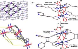
Using a technique called photothermal induced resonance (PTIR), the NIST researchers studied the surface decomposition of OTP films at the nanoscale during curing. PTIR is a novel experimental technique being advanced at NIST that combines the spatial resolution of atomic force microscopy with the chemical specificity of infrared spectroscopy.
The data they gathered suggest that during curing, metal ion clusters are left on the OTP film surface. These ion clusters could act as charge traps, enabling the increased sensitivity. The researchers believe that PTIR characterization will provide important information to link the nanoscale properties of OTP films to the macroscale properties of OTP devices, which may allow the engineering of more efficient OTP-based light detectors and solar cells.
“Discovering that a small applied voltage increases the light sensitivity of hybrid perovskites is extremely exciting,” says Jinsong Huang at the Univ. of Nebraska-Lincoln. “Not only did we add hybrid perovskites to the catalog of light-sensing materials, but the seemingly magical electronic transport capabilities of hybrid perovskites have resulted in better performance with respect to other materials, such as organic and nanocomposite materials, whose sensitivity can be similarly boosted by our strategy.”
Source: NIST
ENTRIES OPEN:
Establish your company as a technology leader. For 50 years, the R&D 100 Awards, widely recognized as the “Oscars of Invention,” have showcased products of technological significance. Learn more.