Research & Development World

  • Home Page
  • Topics
    • Aerospace
    • Archeology
    • Automotive
    • Biotech
    • Chemistry
    • COVID-19
    • Environment
    • Energy
    • Life Science
    • Material Science
    • R&D Market Pulse
    • R&D Management
    • Physics
  • Technology
    • 3D Printing
    • A.I./Robotics
    • Battery Technology
    • Controlled Environments
      • Cleanrooms
      • Graphene
      • Lasers
      • Regulations/Standards
      • Sensors
    • Imaging
    • Nanotechnology
    • Scientific Computing
      • Big Data
      • HPC/Supercomputing
      • Informatics
      • Security
      • Software
    • Semiconductors
  • 2021 R&D 100 Award Winners
    • R&D 100 Awards
    • 2020 Winners
    • Winner Archive
  • Resources
    • Digital Issues
    • Podcasts
    • Subscribe
  • Global Funding Forecast
  • Webinars

Electronics Benefit from Electrons Pairing Off in Semiconductors

By Kayla Wiles, Purdue University | June 21, 2018

The way that electrons paired as composite particles or arranged in lines interact with each other within a semiconductor provides new design opportunities for electronics, according to recent findings in Nature Communications.

What this means for semiconductor components, such as those that send information throughout electronic devices, is not yet clear, but hydrostatic pressure can be used to tune the interaction so that electrons paired as composite particles switch between paired, or “superconductor-like,” and lined-up, or “nematic,” phases. Forcing these phases to interact also suggests that they can influence each other’s properties, like stability — opening up possibilities for manipulation in electronic devices and quantum computing.

“You can literally have hundreds of different phases of electrons organizing themselves in different ways in a semiconductor,” says Gábor Csáthy, Purdue professor of physics and astronomy. “We found that two in particular can actually talk to each other in the presence of hydrostatic pressure.”

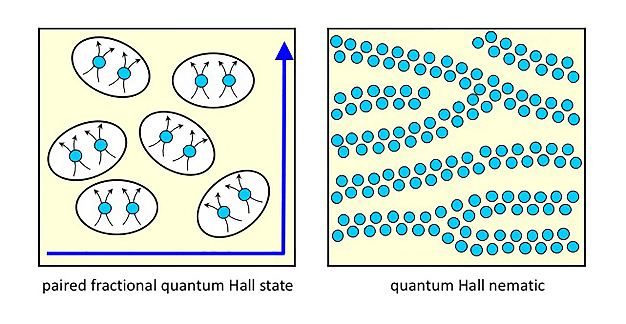
Two different kinds of electron arrangements in a semiconductor, paired as composite particles or lined-up, can interact with and tweak each other in the presence of hydrostatic pressure. Image: Purdue University image/Gábor Csáthy

Csáthy’s group discovered that hydrostatic pressure, which is 10,000 times stronger than ambient pressure, compresses the lattice of atoms in a semiconductor and, therefore, influences the electron arrangement within a two-dimensional electron gas hosted by the semiconductor. The strength of the pressure determines which arrangement is favored and tunes the transition between the paired and lined-up phases, making them more tailorable for an application. Of the two phases, the paired phase may support a certain type of quantum computing.

“We can also tune the interaction by engineering the semiconductor,” Csáthy says. “Say, for example, we grew a semiconductor with a particular width and electron density that we estimated could stabilize the nematic phase. Then we’ve tuned the electron-electron interaction as a result.”

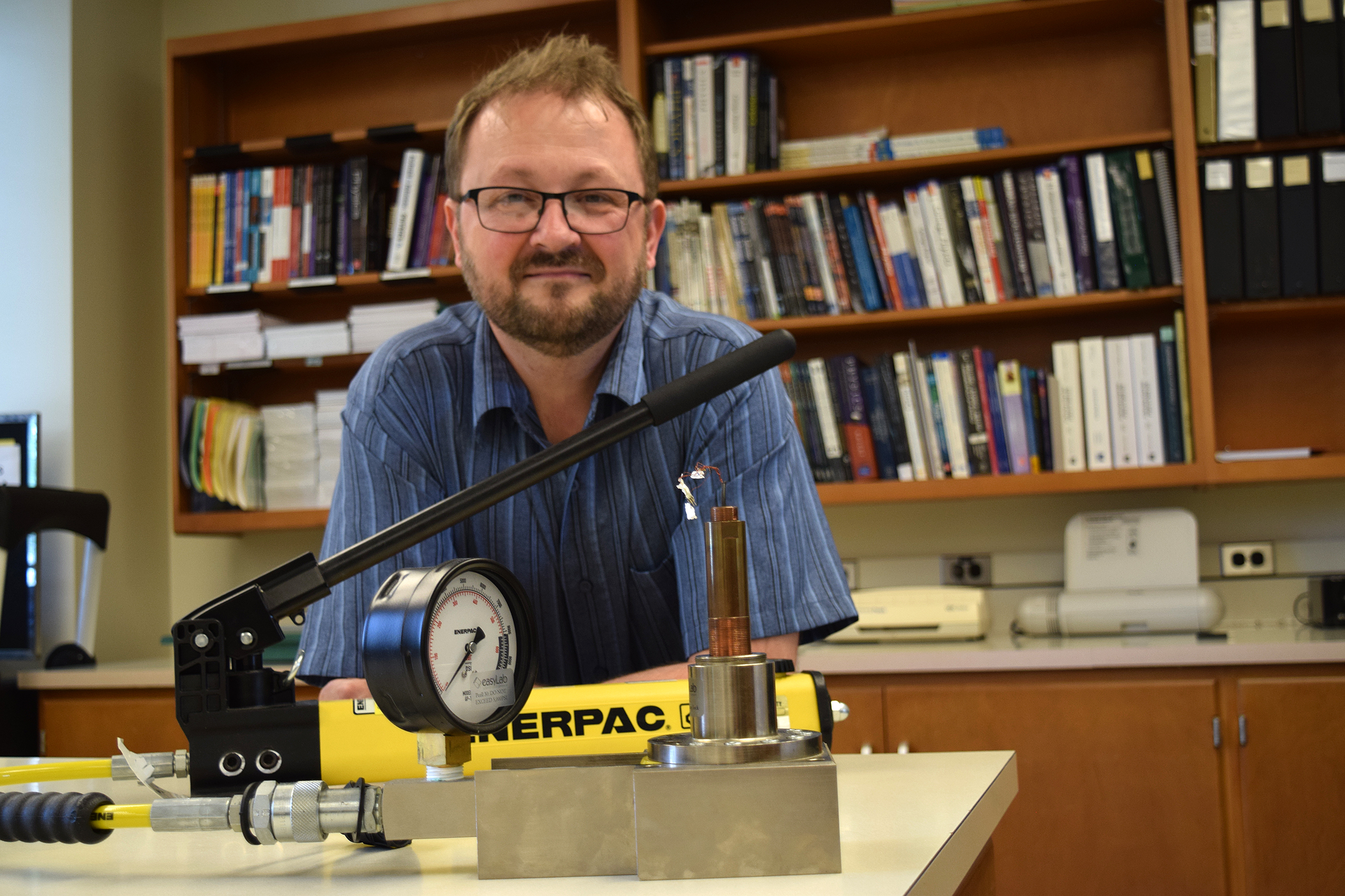
Gábor Csáthy’s lab has discovered a new way that electron arrangements could be manipulated within a two-dimensional electron gas of a semiconductor. Image: Purdue University image/Kayla Wiles

Michael Manfra, Purdue professor of physics and astronomy, electrical and computer engineering and materials engineering, and researchers Loren Pfeiffer and Kenneth West at Princeton University grew the semiconductor samples for this study. Yuli Lyanda-Geller, Purdue associate professor of physics and astronomy, provided theoretical support for the understanding on how these electron-electron interactions took place.

This research was supported by the U.S. Department of Energy, the National Science Foundation, and various fellowships.

Source: Purdue University

Related Articles Read More >

‘Self-driving’ lab speeds up research, synthesis of energy materials
Record-breaking, ultrafast devices step to protecting the grid from EMPs
Surprising semiconductor properties revealed with innovative new method
Thermo Scientific Centrios HX offers precise circuit edit solution for fast prototyping
2021 R&D Global Funding Forecast

Need R&D World news in a minute?

We Deliver!
R&D World Enewsletters get you caught up on all the mission critical news you need in research and development. Sign up today.
Enews Signup

R&D World Digital Issues

February 2020 issue

Browse the most current issue of R&D World and back issues in an easy to use high quality format. Clip, share and download with the leading R& magazine today.

Research & Development World
  • Subscribe to R&D World Magazine
  • Enews Sign Up
  • Contact Us
  • About Us
  • Drug Discovery & Development
  • Pharmaceutical Processing
  • 2022 Global Funding Forecast

Copyright © 2022 WTWH Media LLC. All Rights Reserved. The material on this site may not be reproduced, distributed, transmitted, cached or otherwise used, except with the prior written permission of WTWH Media
Privacy Policy | Advertising | About Us

Search R&D World

  • Home Page
  • Topics
    • Aerospace
    • Archeology
    • Automotive
    • Biotech
    • Chemistry
    • COVID-19
    • Environment
    • Energy
    • Life Science
    • Material Science
    • R&D Market Pulse
    • R&D Management
    • Physics
  • Technology
    • 3D Printing
    • A.I./Robotics
    • Battery Technology
    • Controlled Environments
      • Cleanrooms
      • Graphene
      • Lasers
      • Regulations/Standards
      • Sensors
    • Imaging
    • Nanotechnology
    • Scientific Computing
      • Big Data
      • HPC/Supercomputing
      • Informatics
      • Security
      • Software
    • Semiconductors
  • 2021 R&D 100 Award Winners
    • R&D 100 Awards
    • 2020 Winners
    • Winner Archive
  • Resources
    • Digital Issues
    • Podcasts
    • Subscribe
  • Global Funding Forecast
  • Webinars