 The new wonder material graphene has fantastic properties; for example flexibility, transparency, and high charge carrier mobility. A study by an international team led by David Barbero, assistant professor and group leader at Umeå University in Sweden, shows that semiconducting polymers placed on a layer of graphene transports electrical charge more efficiently than when placed on a substrate of silicon.
The crystallinity of the semiconducting polymers change when they are placed on a graphene substrate compared with when they are placed on silicon, says Barbero. That strongly affects the electronic properties of the materials. Graphene enhances the charge transport through the polymer film, which makes it possible to produce more efficient electronic devices – for example, organic solar cells and OLEDs (organic light emitting diods).
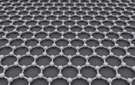
Graphene is a monoatomically thin layer of carbon atoms. Graphene is stronger than steel, but at the same time light and flexible and can transport electrons at lightning speed. That makes the material highly interesting as a component in everything from flexible solar cells to advanced batteries.
In the current study the scientists used synchotron X-ray diffraction to study how crystals are formed in a thin film of semiconducting polymers (plastic) on top of a layer of graphene, and compared it with polymer film on a silicon substrate. The X-ray diffraction was carried out at the National Synchotron Laboratory at Stanford University. The graphene layers were produced at McGill University in Canada, while the ultra-thin polymers and their electronic properties were produced and characterized in David Barbero’s laboratory at Umeå University.
The results, published in the journal Advanced Functional Materials, show that polymer films on graphene results in a much enhanced vertical charge transport compared to films on silicon.
Moreover, a surprising result of this study is that the charge carrier mobility of a thicker polymer film (50 nanometers) was approximately 50 times higher than in the case of an ultra-thin polymer film (10 nanometers) deposited on graphene. A thorough study of the crystallinity of these layers revealed that the ultrathin film formed a well oriented face-on and edge-on lamellae, whereas a thicker film formed a mosaic of lamellae at different angles from the graphene substrate. The crystallites formed at different angles are believed to result in a more efficient vertical charge transport and charge carrier mobility.
These results provide a better understanding of the crystallization of semiconducting polymers on graphene and should help the design of more efficient graphene based organic devices by control of the crystallinity of the semiconducting film, says Barbero.
Release Date: November 25, 2014
Source: Umeå University


