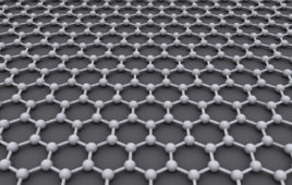
 As electronic components are becoming ever smaller, the industry is gradually approaching the limits of what is achievable using the traditional approach with silicon as a semiconductor material. Graphene, the material with a number of “miraculous” properties, is considered a possible replacement. The one atom thin carbon film is ultra-light, extremely flexible and highly conductive. However, in order to be able to use graphene for electronic components such as field effect transistors, the material has to be “transformed” into a semiconductor. This was achieved by Empa scientists some time ago using a newly developed method — in 2010, they presented, for the first time, graphene nanoribbons (GNR) only a few nanometers wide with precisely shaped edges. For this, the ribbons were grown on a metal surface from specifically designed precursor molecules. The narrower the ribbons, the larger their electronic band gap — i.e. the energy range in which no electrons can be located, which is responsible for ensuring that an electronic switch (for example, a transistor) can be turned on and off. The Empa researchers were then also able to “dope” the nanoribbons, i.e. to furnish the ribbons with impurity atoms such as nitrogen at certain points, in order to influence the electronic properties of the graphene ribbons even more.
In the paper now published in Nature, the Empa team led by Roman Fasel reports, together with colleagues from the Max Planck Institute for Polymer Research in Mainz, headed by Klaus Müllen, and from the Technical University of Dresden led by Xinliang Feng, how it managed to synthesize GNR with perfectly zigzagged edges using suitable carbon precursor molecules and a perfected manufacturing process. The zigzags followed a very specific geometry along the longitudinal axis of the ribbons. This is an important step, because researchers can thus give graphene ribbons different properties via the geometry of the ribbons and especially via the structure of their edges.
As with floor tiling, the right tiles — or precursor molecules — for the synthesis on the surface first had to be found for the specific pattern of the zigzag graphene ribbons. Unlike in organic chemistry, which takes the occurrence of by-products into account on the path to achieving a pure substance, everything had to be designed for the surface synthesis of the graphene ribbons so that only a single product was produced. The scientists repeatedly switched back and forth between computer simulations and experiments, in order to design the best possible synthesis. With molecules in a U-shape, which they allowed to grow together to form a snake-like shape, and additional methyl groups, which completed the zigzag edges, the researchers were able to finally create a “blueprint” for GNR with perfect zigzag edges. To check that the zigzag edges were exact down to the atom, the researchers investigated the atomic structure using an atomic force microscope (AFM). In addition, they were able to characterize the electronic states of the zigzag edges using scanning tunneling spectroscopy (STS).
And these display a very promising feature. Electrons can spin either to the left or to the right, which is referred to as the internal spin of electrons. The special feature of the zigzag GNR is that, along each edge, the electrons all spin in the same direction; an effect which is referred to as ferro-magnetic coupling. At the same time, the so-called antiferromagnetic coupling ensures that the electrons on the other edge all spin in the opposite direction. So the electrons on one side all have a “spin-up” state and on the other edge they all have a “spin-down” state.
Thus, two independent spin-channels with opposite “directions of travel” arise on the band edges, like a road with separated lanes. Via intentionally integrated structural defects on the edges or — more elegantly — via the provision of an electrical, magnetic or optical signal from the outside, spin barriers and spin filters can thus be designed that require only energy in order to be switched on and off — the precursor to a nanoscale and also extremely energy efficient transistor.
Possibilities such as this make GNR extremely interesting for spintronic devices; these use both the charge and the spin of the electrons. This combination is prompting scientists to forecast completely new components, e.g. addressable magnetic data storage devices which maintain the information that has been fed in even after the power has been turned off.
Source: Empa


