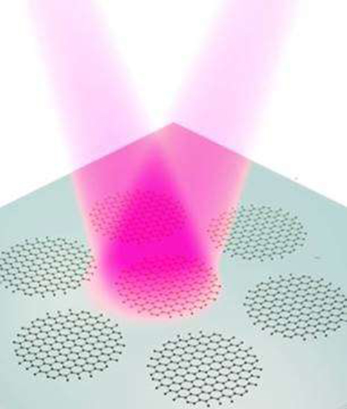
Probing graphene plasmon in nanodisks by FTIR. (Credit: Xiaolong Zhu from DTU Nanotech)
Graphene’s unique properties can be both a blessing and a curse to researchers, especially to those at the intersection of optical and electronic applications. These single-atom thick sheets feature highly mobile electrons on their flexible profiles, making them excellent conductors, but in general graphene sheets do not interact with light efficiently.
Problematic for shorter wavelength light, photons in the near infrared region of the spectrum, where telecommunication applications become realizable. In a paper published this week in the journal Optics Letters, from The Optical Society (OSA), researchers at the Technical University of Denmark have demonstrated, for the first time, efficient absorption enhancement at a wavelength of 2 micrometers by graphene, specifically by the plasmons of nanoscale graphene disks.
Much like water ripples arising from the energy of a dropped pebble, electronic oscillations can arise in freely moving conduction electrons by absorbing light energy. The resulting collective, coherent motions of these electrons are called plasmons, which also serve to amplify the strength of the absorbed light’s electric field at close proximity. Plasmons are becoming increasingly commonplace in various optoelectronic applications where highly conductive metals can be easily integrated.
Graphene plasmons, however, face an extra set of challenges unfamiliar to the plasmons of bulk metals. One of these challenges is the relatively long wavelength needed to excite them. Many efforts taking advantage of the enhancing effects of plasmons on graphene have demonstrated promise, but for low energy light.
“The motivation of our work is to push graphene plasmons to shorter wavelengths in order to integrate graphene plasmon concepts with existing mature technologies,” said Sanshui Xiao, associate professor from the Technical University of Denmark.
To do so, Xiao, Wang and their collaborators took inspiration from recent developments at the university’s Center of Nanostructured Graphene (CNG), where they demonstrated a self-assembly method resulting in large arrays of graphene nanostructures. Their method primarily uses geometry to bolster the graphene plasmon effects at shorter wavelengths by decreasing the size of the graphene structures.
Using lithographic masks prepared by a block copolymer based self-assembly method, the researchers made arrays of graphene nanodisks. They controlled the final size of the disks by exposing the array to oxygen plasma which etched away at the disks, bringing the average diameter down to approximately 18 nm. This is approximately 1000 times smaller than the width of a human hair.
The array of approximately 18 nm disks, resulting from 10 seconds of etching with oxygen plasma, showed a clear resonance with 2 micrometer wavelength light, the shortest wavelength resonance ever observed in graphene plasmons.
An assumption might be that longer etching times or finer lithographic masks, and therefore smaller disks, would result in even shorter wavelengths. Generally speaking this is true, but at 18 nm the disks already start requiring consideration of atomic details and quantum effects.
Instead, the team plans to tune graphene plasmon resonances at smaller scales in the future using electrical gating methods, where the local concentration of electrons and electric field profile alter resonances.
Xiao said, “To further push graphene plasmons to shorter wavelengths, we plan to use electrical gating. Instead of graphene disks, graphene antidots (i.e. graphene sheets with regular holes) will be chosen because it is easy to implement a back-gating technique.”
There are also fundamental limits to the physics that prevent shortening the graphene plasmon resonance wavelength with more etching. “When the wavelength becomes shorter, the interband transition will soon play a key role, leading to broadening of the resonance. Due to weak coupling of light with graphene plasmons and this broadening effect, it will become hard to observe the resonance feature,” Xiao explained.


