Photonic nanostructures can be used for many applications, not just in solar cells, but also in optical sensors for cancer markers or other biomolecules, for example.
A team at Helmholtz-Zentrum Berlin using computer simulations and machine learning has now shown how the design of such nanostructures can be selectively optimized.
The results are published in Communications Physics.
Nanostructures can increase the sensitivity of optical sensors enormously — provided that the geometry meets certain conditions and matches the wavelength of the incident light. This is because the electromagnetic field of light can be greatly amplified or reduced by the local nanostructure.
The HZB Young Investigator Group “Nano-SIPPE” headed by Professor Christiane Becker is working to develop these kinds of nanostructures. Computer simulations are an important tool for this.
Dr. Carlo Barth from the Nano-SIPPE team has now identified the most important patterns of field distribution in a nanostructure using machine learning, and has thereby explained the experimental findings very well for the first time.
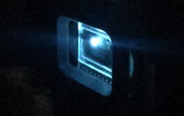
The photonic nanostructures examined in this paper consist of a silicon layer with a regular hole pattern coated with what are referred to as quantum dots made of lead sulphide.
Excited with a laser, the quantum dots close to local field amplifications emit much more light than on an unordered surface. This makes it possible to empirically demonstrate how the laser light interacts with the nanostructure.
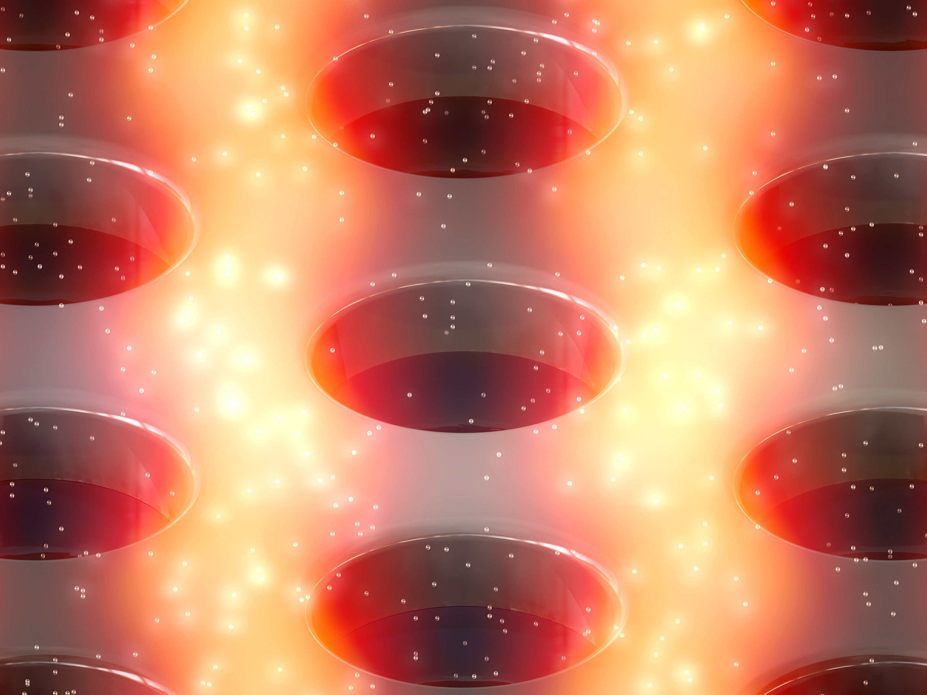
The computer simulation shows how the electromagnetic field is distributed in the silicon layer with hole pattern after excitation with a laser. Here, stripes with local field maxima are formed, so that quantum dots shine particularly strongly. Image: C. Barth/HZB
In order to systematically record what happens when individual parameters of the nanostructure change, Barth calculates the three-dimensional electric field distribution for each parameter set using software developed at the Zuse Institute Berlin.
Barth then had these enormous amounts of data analyzed by other computer programs based on machine learning.
“The computer has searched through the approximately 45,000 data records and grouped them into about 10 different patterns,” he explains.
Finally, Barth and Becker succeeded in identifying three basic patterns among them in which the fields are amplified in various specific areas of the nanoholes.
This allows photonic crystal membranes based on excitation amplification to be optimized for virtually any application. This is because some biomolecules accumulate preferentially along the hole edges, for example, while others prefer the plateaus between the holes, depending on the application.
With the correct geometry and the right excitation by light, the maximum electric field amplification can be generated exactly at the attachment sites of the desired molecules.
This would increase the sensitivity of optical sensors for cancer markers to the level of individual molecules, for example.
Source: Helmholtz-Zentrum Berlin