We conclude our discussion of NEMS and MEMS with a potpourri of techniques including an additional MEMS based sensing tool, a modeling technique for predicting the effects of contamination in MEMS devices, approaches to avoiding contamination in MEMS and NEMS devices, and applications of nano-technology approaches to contamination minimization at the macroscopic level.
Shear force microscopy
As discussed last month, atomic force microscopy (AFM) sensors detect surface defects including particulate contamination. However, microscopic device manufacturers face additional surface issues including friction between contacting or near contacting parts of the device. While conventional AFM measures small displacements of the probe perpendicular to the surface, a somewhat similar device, known as Shear Force Microscopy (SFM or ShFM), or sometimes referred to as Transverse Dynamic Force Microscopy (TDFM) uses a cantilever probe moving parallel to the surface. It is never in actual contact with the surface but is affected by the dissipative forces associated with friction.1 In a sense, SFM measures the lubricity or “stickiness” of the surface. It is particularly useful for the study of softer materials and also enables non-destructive, high resolution topography imaging of delicate samples such asthin layers of organic molecules.
Modeling effects of contamination
Suppose you are designing a microdevice. It would be very useful to predict the effects of contamination or defects on performance. The proposed device design might be modified to minimize such effects. Researchers at the Carnegie-Mellon University have developed a computer modeling tool called CARAMEL (Contamination And Reliability Analysis of MicroElectromechanical Layout) which is being used to analyze the predicted impact of contamination particles on the structural and material properties of MEMS.2 Given MEMS design, a particulate description, and a process (fabrication) recipe, CARAMEL performs a process simulation and creates a three-dimensional representation of the resulting defective structure. The CARAMEL output can then be used as part of the input to the Finite Element Analysis (FEA), a computerized analysis tool that analyzes how various parts of a structure will interact, including expected stresses and strains. Thus CARAMEL allows designers to identify specific potential areas of vulnerability without incurring the costs of prototype development.
Preventing contamination in MEMS and NEMS devices
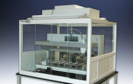
MEMS or NEMS devices are especially vulnerable to damage during latter stages of fabrication. It is not uncommon for the back end of the MEMS product flow to represent 80% or more of the total cost.3 The presence of mechanical structures on the surface adds fragility. For example, many MEMS devices are produced on a wafer; and pre-packaging steps, such as wafer dicing, may introduce contamination or damage. Surface contamination can lead to impaired performance.
A number of techniques have been developed to protect micro-mechanical devices. Encapsulation techniques include a “Near” hermetic package of molded liquid crystal polymer, designed to provide protection but at a reasonable cost.
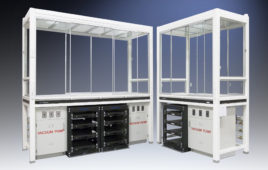
A second technique has been developed to protect MEMS vacuum devices. Macroscopic vacuum devices frequently use getters to maintain high vacuum conditions. Getters contain molecules with a high affinity for gaseous contaminants, sweeping them out of the cavity (a bit like flypaper). Unfortunately, traditional sintered metal getters can themselves be a major source of particulate contamination that can migrate into the mechanical regions of the MEMS device.5 A thin-film getter known as NanoGetter™ is a more appropriate solution for MEMS vacuum devices by providing the gettering function without particle generation. Nano-technology approaches to preventing contamination of macroscopic structures
Nano-technology approaches to preventing contamination of macroscopic structures
Sometimes the best protection from contaminates are other contaminates. Two nano-technology techniques are being commercially developed with potential application to consumer products. Nano-structures have been developed that mimic the hydrophobic (water repelling) properties of the lotus plant.6 The precursors of these structures are supplied as an aerosol spray coating containing hydrophobic polymers such as polypropylene, polyethylene, and waxes. As it dries, the coating forms a nanostructure through self-assembly. Although current target applications are consumer products including paper and leather, similar techniques could be developed to protect microscopic devices or for other fabrication applications.
A somewhat similar approach is employed for “self-cleaning” glass.7 An extremely thin (~40nm) coating of titanium dioxide provides both a hydrophilic property as well as a catalytic property that causes solar UV light to break down organic contaminants on the surface. The surface has an exceedingly high contact angle, on the order of 140 degrees. The surface is effectively soiled with a specific contaminate. As a result, water sheets right off, carrying dirt particles with it.
References:
1 K. Karrai, I. Tiemann. Phys. Rev. B, Vol. 62, No. 19, (2000) p. 13174.
2 A. Kolpekwar, T. Jiang, R. D. Blanton’ Journal Of Microelectromechanical Systems, Vol. 8, No. 3, (1999) p. 309.
3 R. Markunas. A2C2 Magazine, (February, 2003).
4 Flipchips.com, tutorial #36.
5 D. Sparks, S. Massoud-Ansari, N. Najafi. IEEE Transactions on Advanced Packaging, Vol. 26, No. 3, (August 2003).
6 Nanotechweb.org, 11/8/02 BASF Lotus-Effect™.
7 Nanotechweb.org, (09/19/02).