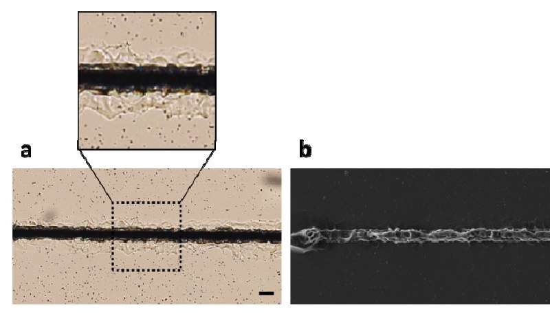
Using a one-step laser fabrication process, researchers created flexible hybrid microwires that conduct electricity. (a) An optical microscope image of the silver (black) and silicone (clear) microwires. (b) Scanning electron microscopy image of the same fabricated structure. Both scale bars are equal to 25 microns. Credit: Mitsuhiro Terakawa, Keio University
Scientists have created new microstructures that could pave the way for new flexible optical and electrical devices.
Researchers from Keio University in Japan have developed a single-step, laser-based method to produce small, precise hybrid microstructures of silver and flexible silicone that could enable factories to mass-produce customized devices that combine soft materials, like engineered tissue, with hard materials that add functions, like glucose sensing.
“These types of microstructures could possibly be used to measure very small movements or changes, such as a slight movement from an insect’s body or the subtle expression produced by a human facial muscle,” research team leader Mitsuhiro Terakawa from Keio University, said in a statement. “This information could be used to create perfect computer-generated versions of these movements.”
The researchers produced wire-like structures of silver and surrounded them with a type of silicone called polydimethylsiloxane (PDMS), which was used because it is flexible and biocompatible.
The structures—which measure as little as 25 microns wide—were fabricated by irradiating a mixture of PDMS and silver ions with extremely short laser pulses that last just femtoseconds.
“We believe we are the first group to use femtosecond laser pulses to create a hybrid material containing PDMS, which is very useful because of its elasticity,” Terakawa said. “The work represents a step towards using a single, precision laser processing technology to fabricate biocompatible devices that combine hard and soft materials.”
The one-step fabrication method used to make the hybrid microstructures combines the light-based chemical reactions known as photopolymerization and photoreduction, both of which were induced using femtosecond laser pulses. Photopolymerization uses light to harden a polymer, and photoreduction uses light to form microstructures and nanostructures from metal ions.
The researchers created the wire microstructures by irradiating the PDMS-silver mixture with light from femtosecond laser emitting at 522-nm.
They discovered that just one laser scan formed wires that exhibited both the electrical conductivity of metal and the elasticity of a polymer.
Additional scans could also be used to produce thicker and more uniform structures and they also showed that the wire structures responded to mechanical force by blowing air over the structures to create a pressure of three kilopascals.
The researcher also say the approach could be used to make minute 3D metal-silicone structures and they plan to examine whether the fabricated wires maintain their structure and properties over time.
“Our work demonstrates that simultaneously inducing photoreduction and photopolymerization is a promising method for fabricating elastic and electrically conductive microstructures,” Terakawa said. “This is one step toward our long-term goal of developing a smart factory for fabricating many human-compatible devices in one production line, whether the materials are soft or hard.”
The study was published in Optical Materials Express.


