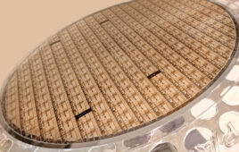
 Many semiconductor devices in modern technology — from integrated circuits to solar cells and LEDs — are based on nanostructures. Producing arrays of regular nanostructures usually requires substantial effort. If they were self-organized, the production of such devices would be considerably faster and the costs would therefore sink. Dr. Stefan Facsko from the Helmholtz-Zentrum Dresden-Rossendorf (HZDR), and Dr. Xin Ou from the Shanghai Institute of Microsystem and Information Technology (SIMIT), Chinese Academy of Sciences, have now demonstrated a method for self-organization of nanostructured arrays via broad ion beam irradiation. The results have been published in the scientific journal Nanoscale.
In their astounding method, the researchers use ion beams, which are fast, electrically charged atoms. They direct a broad beam of noble gas ions onto a gallium arsenide wafer, which, for example, is used in producing high-speed and high-frequency transistors, photocells or light-emitting diodes.
“One could compare ion bombardment with sand blasting. This means that the ions mill off the surface of the target. There, the desired nanostructures are created all by themselves,” explains Facsko. The finely chiseled and regular structure is reminiscent of sand dunes, natural structures created by wind. It all occurs, however, in a nano-realm, with a mere distance of fifty nanometers between two dunes — strands of human hair are two thousand times thicker.
At room temperature, however, the ion beam destroys the crystal structure of the gallium arsenide and thus its semiconducting properties. Facsko’s group at the HZDR’s Ion Beam Center therefore uses the opportunity to heat the sample during ion bombardment. At about four hundred degrees Celsius, the destroyed structures recover rapidly. A further effect ensures that the nano-dunes on the semiconductor surface develop. The colliding ions not only shift the atoms they hit, but also knock individual atoms entirely out of the crystal structure. Since the volatile arsenic does not remain bound on the surface, the surface soon consists only of gallium atoms. In order to compensate for the missing arsenic atom bonds, pairs of two gallium atoms form, which arrange themselves in long rows. If the ion beam knocks out further atoms next to them, the gallium pairs cannot slip down the step that has been created because the temperatures are too low for this to happen. This is how the long rows of gallium pairs form nano-dunes after a period of time, in which several long pairs of lines lie next to each other.
Many experiments at different temperatures and comprehensive computations were necessary to both preserve the crystalline state of the semiconducting material as well to produce the well-defined structures at the nanoscale. Facsko says, “The method of inverse epitaxy works for various materials but is still in its basic research phase. Because we use particularly low energy ions — under 1 kilovolt — which can be generated using simple methods, we hope that we can point the way for industrial implementation. The manufacturing of similar structures with current state of the art methods needs considerably more effort.”
Release Date: September 8, 2015
Source: Helmholtz-Zentrum Dresden-Rossendorf


