Research & Development World

  • R&D World Home
  • Topics
    • Aerospace
    • Automotive
    • Biotech
    • Careers
    • Chemistry
    • Environment
    • Energy
    • Life Science
    • Material Science
    • R&D Management
    • Physics
  • Technology
    • 3D Printing
    • A.I./Robotics
    • Software
    • Battery Technology
    • Controlled Environments
      • Cleanrooms
      • Graphene
      • Lasers
      • Regulations/Standards
      • Sensors
    • Imaging
    • Nanotechnology
    • Scientific Computing
      • Big Data
      • HPC/Supercomputing
      • Informatics
      • Security
    • Semiconductors
  • R&D Market Pulse
  • R&D 100
    • Call for Nominations: The 2025 R&D 100 Awards
    • R&D 100 Awards Event
    • R&D 100 Submissions
    • Winner Archive
    • Explore the 2024 R&D 100 award winners and finalists
  • Resources
    • Research Reports
    • Digital Issues
    • R&D Index
    • Subscribe
    • Video
    • Webinars
  • Global Funding Forecast
  • Top Labs
  • Advertise
  • SUBSCRIBE

Nanometer-Thin Layer Improves Semiconductor Efficiency

By Max Planck Institute for Polymer Research | March 12, 2018

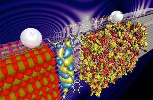
Visualization of a current through an OLED, flowing via a thin molecular layer (center) from an electrode (left) to an organic semiconductor (right). © Max Planck Institute for Polymer Research

Organic light-emitting diodes (OLEDs) are used as light sources in high-quality smartphone displays and large-area high-end products such as OLED televisions. The main active component in an OLED is a light-emitting layer of an organic semiconductor, which converts electrical energy into visible light. In an OLED, the organic semiconducting layer is situated between two electrodes; by applying a voltage across these two electrodes, an electric current passes through the OLED, which is converted into visible light.

However, for many organic semiconductors, especially for blue- or ultraviolet-emitting materials, it is difficult to inject the current from the positive electrode into the OLED. This leads to low efficiencies in OLEDs.

Dr. Gert-Jan Wetzelaer, Group Leader at the Max Planck Institute for Polymer Research in Mainz, Germany, has recently discovered a way of improving the current injection from the positive electrode in OLEDs. Wetzelaer and his team have covered the positive electrode with an ultrathin layer of another organic semiconductor as a spacer layer between the electrode and the light-emitting organic semiconductor.

Wetzelaer says, “The result was unexpected. This nanometer-thin layer facilitates charge transfer between the electrode and the organic semiconductor. Although it seems to be illogical at first, eliminating physical contact between electrode and semiconductor actually improves the electrical contact.”

Improving electrical contact with an ultrathin interlayer greatly increases the efficiency of ultraviolet-emitting OLEDs. The scientists at the MPI for Polymer Research have demonstrated this improvement of electrodes for a large number of organic semiconductors and for different spacer layers. Professor Paul Blom, Director at the Max Planck Institute for Polymer Research and head of its Molecular Electronics Department, is convinced: “This simple method of covering electrodes in OLEDs with an ultrathin layer for current-injection improvement is a resounding success for technical application in high-end electronics.”

Gert-Jan Wetzelaer and his research team are very confident that this new approach for fabricating improved contacts can be used in basically any organic-semiconductor device, which could boost their performance now.

Source: Max Planck Institute for Polymer Research

Related Articles Read More >

TSMC’s N3P hits mass production, with N3X customer sampling slated for Q3–Q4 2025a
7 major R&D developments this week: Tariff uncertainty persists, Pfizer sells campus, Scania acquires Northvolt unit
While Trump tariffs spare phones/PCs, R&D could faces GPU cost pressures
Why IBM predicts quantum advantage within two years
rd newsletter
EXPAND YOUR KNOWLEDGE AND STAY CONNECTED
Get the latest info on technologies, trends, and strategies in Research & Development.
RD 25 Power Index

R&D World Digital Issues

Fall 2024 issue

Browse the most current issue of R&D World and back issues in an easy to use high quality format. Clip, share and download with the leading R&D magazine today.

Research & Development World
  • Subscribe to R&D World Magazine
  • Enews Sign Up
  • Contact Us
  • About Us
  • Drug Discovery & Development
  • Pharmaceutical Processing
  • Global Funding Forecast

Copyright © 2025 WTWH Media LLC. All Rights Reserved. The material on this site may not be reproduced, distributed, transmitted, cached or otherwise used, except with the prior written permission of WTWH Media
Privacy Policy | Advertising | About Us

Search R&D World

  • R&D World Home
  • Topics
    • Aerospace
    • Automotive
    • Biotech
    • Careers
    • Chemistry
    • Environment
    • Energy
    • Life Science
    • Material Science
    • R&D Management
    • Physics
  • Technology
    • 3D Printing
    • A.I./Robotics
    • Software
    • Battery Technology
    • Controlled Environments
      • Cleanrooms
      • Graphene
      • Lasers
      • Regulations/Standards
      • Sensors
    • Imaging
    • Nanotechnology
    • Scientific Computing
      • Big Data
      • HPC/Supercomputing
      • Informatics
      • Security
    • Semiconductors
  • R&D Market Pulse
  • R&D 100
    • Call for Nominations: The 2025 R&D 100 Awards
    • R&D 100 Awards Event
    • R&D 100 Submissions
    • Winner Archive
    • Explore the 2024 R&D 100 award winners and finalists
  • Resources
    • Research Reports
    • Digital Issues
    • R&D Index
    • Subscribe
    • Video
    • Webinars
  • Global Funding Forecast
  • Top Labs
  • Advertise
  • SUBSCRIBE