Nanotechnology Leads to Discovery of Super Superconductors
University of California scientists working at Los Alamos National Laboratory with a researcher from the University of Cambridge have demonstrated a simple and industrially scaleable method for improving the current densities of superconducting coated conductors in magnetic field environments. The discovery has the potential to increase the already impressive carrying capacity of superconducting wires and tapes by as much as 200 to 500 percent in certain uses, like motors and generators, where high magnetic fields diminish current densities.
In research reported in the journal Nature Materials, University of Cambridge scientist Judith Macmanus-Driscoll and her Los Alamos colleagues discovered that when the compound barium zirconate is deposited simultaneously with the yttrium-barium-copper-oxide superconductor it naturally forms nanoscale particles embedded in superconductor films. The result was a two to five fold increase in the current densities of coated conductors in high magnetic fields operating at liquid nitrogen temperatures.
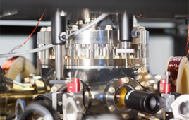
Superconducting wires and tapes carry hundreds of times more electrical current than conventional copper wires with little or no electrical resistance. Superconducting technology is poised to bring substantial energy efficiencies to electrical power transmission systems in the United States. Much of the excitement caused by this discovery is due to the fact that the process can be easily and economically incorporated into commercial processing of the superconductors. The advance is important for the development of powerful, energy efficient superconducting electric motors and generators for civilian and military applications. The Laboratory conducts research and development of high-temperature superconducting tapes under the auspices of Los Alamos Superconductivity Technology Center (STC).
Dean Peterson, leader of the STC, said, “This is a significant technical advancement because it means we are now beginning to understand how to control defects in these superconducting materials and use them to our advantage. This was the first time we have been able to control the structural defects and in doing so, better engineer the material’s structure to optimize performance.”
Contrary to what one might think, the presence of certain types of defects in the superconducting film is not a problem, but a necessity. Early high temperature superconductivity research had the goal of eliminating large-scale defects, which effectively blocked the flow of electrical currents through the material. This required an ordering of superconducting grains, much like the bricks in a smooth road, allowing the unimpeded flow of high-density electrical currents. Scientists later discovered that small, nanoscale defects are required to maintain high current densities in superconductors, particularly in the presence of high magnetic fields. Nanoscale refers to defect sizes roughly 50-100 atoms across.
Because magnetic fields create small swirls of current in a superconductor called vortices, much like tornadoes in the air, that move through the material under the influence of electrical currents causing resistance to the flow of the current, the nanoscale defects immobilize or “pin” the vortices allowing the current to flow without resistance. These nanoscale defects can come in various forms ranging from small particles to flat plates and long string-like objects. Previous attempts to produce dense arrays of these types of small-scale defects, such as irradiation by fast heavy ions, were impractical for commercial production or difficult to control in a reproducible manner.
In addition to Macmanus-Driscoll and Peterson, other members of the team included Stephen Foltyn, Quanxi Jia, Haiyan Wang, Adriana Serquis, Leonardo Civale, Boris Maiorov, Marilyn Hawley and Martin Maley, all of Los Alamos. The research was conducted under the auspices of the Los Alamos Superconductivity Technology Center and was funded by the DOE’s Office of Electric Transmission and Distribution.