Single-walled carbon nanotubes are loaded with desirable properties. In particular, the ability to conduct electricity at high rates of speed makes them attractive for use as nanoscale transistors. But this and other properties are largely dependent on their structure, and their structure is determined when the nanotube is just beginning to form.
In a step toward understanding the factors that influence how nanotubes form, researchers at the National Institute of Standards and Technology (NIST), the University of Maryland, and Texas A&M have succeeded in filming them when they are only a few atoms old. These nanotube “baby pictures” give crucial insight into how they germinate and grow, potentially opening the way for scientists to create them en masse with just the properties that they want.
The results were published online in Nano Letters.
To better understand how carbon nanotubes grow and how to grow the ones you want, you need to understand the very beginning of the growth process, called nucleation. To do that, you need to be able to image the nucleation process as it happens. However, this is not easy because it involves a small number of fast-moving atoms, meaning you have to take very high resolution pictures very quickly.
Because fast, high-resolution cameras are expensive, NIST scientists instead slowed the growth rate by lowering the pressure inside their instrument, an environmental scanning transmission electron microscope. Inside the microscope’s chamber, under high heat and low pressure, the team watched as carbon atoms generated from acetylene rained down onto 1.2-nanometer bits of cobalt carbide, where they attached, formed into graphene, encircled the nanoparticle, and began to grow into nanotubes.
“Our observations showed that the carbon atoms attached only to the pure metal facets of the cobalt carbide nanoparticle, and not those facets interlaced with carbon atoms,” says NIST chemist Renu Sharma, who led the research effort. “The burgeoning tube then grew above the cobalt-carbon facets until it found another pure metal surface to attach to, forming a closed cap. Carbon atoms continued to attach at the cobalt facets, pushing the previously formed graphene along toward the cap in a kind of carbon assembly line and lengthening the tube. This whole process took only a few seconds.”
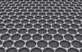
According to Sharma, the carbon atoms seek out the most energetically favorable configurations as they form graphene on the cobalt carbide nanoparticle’s surface. While graphene has a mostly hexagonal, honeycomb-type structure, the geometry of the nanoparticle forces the carbon atoms to arrange themselves into pentagonal shapes within the otherwise honeycomb lattice. Crucially, these pentagonal irregularities in the graphene’s structure are what allows the graphene to curve and become a nanotube.
Because the nanoparticles’ facets also appear to play a deciding role in the nanotube’s diameter and chirality, or direction of twist, the group’s next step will be to measure the chirality of the nanotubes as they grow. The group also plans to use metal nanoparticles with different facets to study their adhesive properties to see how they affect the tubes’ chirality and diameter.
Release Date: December 1, 2014
Source: NIST


