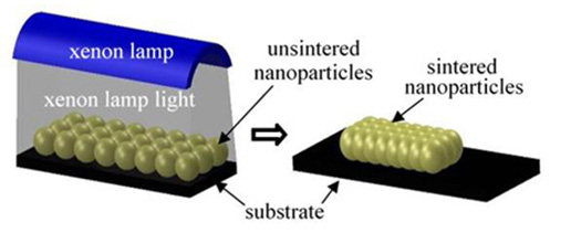
Fusing, or sintering, nanoparticles by exposing them to pulses of intense light from a xenon lamp. Image: Rajiv Malhotra/Rutgers University-New Brunswick
Engineers at Rutgers University-New Brunswick and Oregon State University are developing a new method of processing nanomaterials that could lead to faster and cheaper manufacturing of flexible, thin film devices — from touch screens to window coatings, according to a new study.
The “intense pulsed light sintering” method uses high-energy light over an area nearly 7,000 times larger than a laser to fuse nanomaterials in seconds. Nanomaterials are materials characterized by their tiny size, measured in nanometers. A nanometer is one millionth of a millimeter, or about 100,000 times smaller than the diameter of a human hair.
The existing method of pulsed light fusion uses temperatures of around 250 degrees Celsius (482 degrees Fahrenheit) to fuse silver nanospheres into structures that conduct electricity. But the new study, published in RSC Advances and led by Rutgers School of Engineering doctoral student Michael Dexter, showed that fusion at 150 degrees Celsius (302 degrees Fahrenheit) works well while retaining the conductivity of the fused silver nanomaterials.
The engineers’ achievement started with silver nanomaterials of different shapes: long, thin rods called nanowires in addition to nanospheres. The sharp reduction in temperature needed for fusion makes it possible to use low-cost, temperature-sensitive plastic substrates like polyethylene terephthalate (PET) and polycarbonate in flexible devices, without damaging them.
“Pulsed light sintering of nanomaterials enables really fast manufacturing of flexible devices for economies of scale,” says Rajiv Malhotra, the study’s senior author and assistant professor in the Department of Mechanical and Aerospace Engineering at Rutgers-New Brunswick. “Our innovation extends this capability by allowing cheaper temperature-sensitive substrates to be used.”
Fused silver nanomaterials are used to conduct electricity in devices such as radio-frequency identification (RFID) tags, display devices and solar cells. Flexible forms of these products rely on fusion of conductive nanomaterials on flexible substrates, or platforms, such as plastics and other polymers.
“The next step is to see whether other nanomaterial shapes, including flat flakes and triangles, will drive fusion temperatures even lower,” Malhotra says.
In another study, published in Scientific Reports, the Rutgers and Oregon State engineers demonstrated pulsed light sintering of copper sulfide nanoparticles, a semiconductor, to make films less than 100 nanometers thick.
“We were able to perform this fusion in two to seven seconds compared with the minutes to hours it normally takes now,” says Malhotra, the study’s senior author. “We also showed how to use the pulsed light fusion process to control the electrical and optical properties of the film.”
Their discovery could speed up the manufacturing of copper sulfide thin films used in window coatings that control solar infrared light, transistors and switches, according to the study. This work was funded by the National Science Foundation and The Walmart Manufacturing Innovation Foundation.
Source: Rutgers University


