Research & Development World

  • R&D World Home
  • Topics
    • Aerospace
    • Automotive
    • Biotech
    • Careers
    • Chemistry
    • Environment
    • Energy
    • Life Science
    • Material Science
    • R&D Management
    • Physics
  • Technology
    • 3D Printing
    • A.I./Robotics
    • Software
    • Battery Technology
    • Controlled Environments
      • Cleanrooms
      • Graphene
      • Lasers
      • Regulations/Standards
      • Sensors
    • Imaging
    • Nanotechnology
    • Scientific Computing
      • Big Data
      • HPC/Supercomputing
      • Informatics
      • Security
    • Semiconductors
  • R&D Market Pulse
  • R&D 100
    • 2025 R&D 100 Award Winners
    • 2025 Professional Award Winners
    • 2025 Special Recognition Winners
    • R&D 100 Awards Event
    • R&D 100 Submissions
    • Winner Archive
  • Resources
    • Research Reports
    • Digital Issues
    • Educational Assets
    • R&D Index
    • Subscribe
    • Video
    • Webinars
    • Content submission guidelines for R&D World
  • Global Funding Forecast
  • Top Labs
  • Advertise
  • SUBSCRIBE

New Method Promises Easier Nanoscale Manufacturing

By Louise Lerner, University of Chicago | July 28, 2017

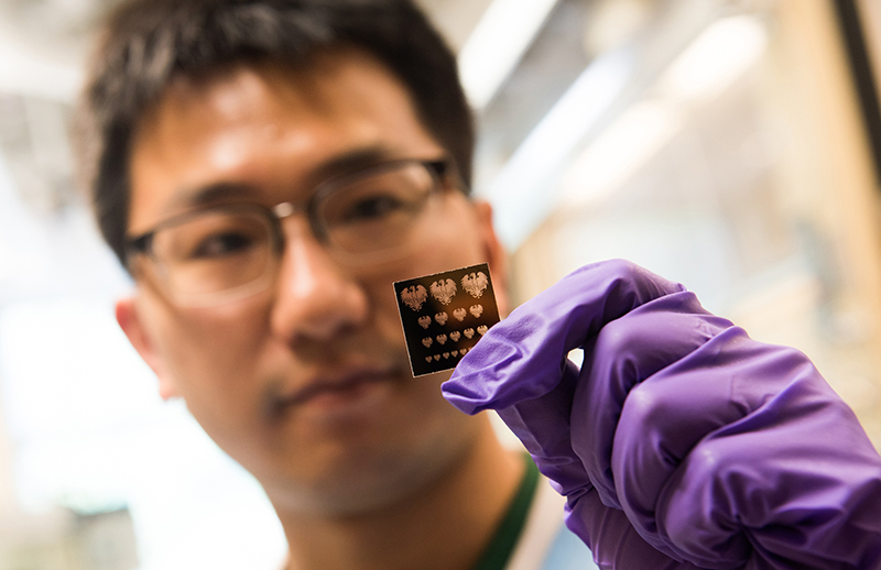
Postdoctoral researcher Yuanyuan Wang holds a ‘mask’ used in a new process that makes it easier to build nanomaterials into transistors, solar cells and other devices. Photo by Jean Lachat

Scientists at the University of Chicago and Argonne National Laboratory have discovered a new way to precisely pattern nanomaterials that could open a new path to the next generation of everyday electronic devices.

The new research, published in Science, is expected to make such materials easily available for eventual use in everything from LED displays to cellular phones to photodetectors and solar cells. Though nanomaterials are promising for future devices, ways to build them into complex structures have been limited and small-scale.

“This is a step needed to move quantum dots and many other nanomaterials from proof-of-concept experiments to real technology we can use,” said co-author Dmitri Talapin, professor of chemistry at UChicago and a scientist with the Center for Nanoscale Materials at Argonne. “It really expands our horizons.”

The foundation of modern computing is a tiny switch called the transistor, made billions at a time by a technique called photolithography. This process, which has made smartphones cheap and ubiquitous, carves a stencil out of a layer of organic polymer by laying down a patterned “mask” and illuminating it with ultraviolet light. After the new material is deposited on top, the polymer stencil is lifted off to reveal the pattern. Several rounds of such patterning build a miniature transistor onto the material.

But the method has its limitations. Only a few materials can be patterned this way; it was originally developed for silicon, and as silicon’s half-century reign over electronics reaches its end, scientists are looking ahead to the next materials.

One such avenue of interest is nanomaterials—tiny crystals of metals or semiconductors. At this scale, they can have unique and useful properties, but manufacturing devices out of them has been difficult.

The new technique, called DOLFIN, makes different nanomaterials directly into “ink” in a process that bypasses the need to lay down a polymer stencil. Talapin and his team carefully designed chemical coatings for individual particles. These coatings react with light, so if you shine light through a patterned mask, the light will transfer the pattern directly into the layer of nanoparticles below—wiring them into useful devices.

“We found the quality of the patterns was comparable to those made with state-of-the-art techniques,” said lead author Yuanyuan Wang, postdoctoral researcher at UChicago. “It can be used with a wide range of materials, including semiconductors, metals, oxides or magnetic materials—all commonly used in electronics manufacturing.”

The team is working toward commercializing the DOLFIN technology in partnership with UChicago’s Polsky Center for Entrepreneurship and Innovation.

SOURCE: University of Chicago

Related Articles Read More >

CEA-Leti achieves 400°C CMOS fabrication milestone for 3D chip stacking
The 2025 R&D 100 Finalists are here
New nanotechnology method increases microalgae biofuel yield by 300%
New nanopore sensor paves the way for fast, accurate, low-cost DNA sequencing
rd newsletter
EXPAND YOUR KNOWLEDGE AND STAY CONNECTED
Get the latest info on technologies, trends, and strategies in Research & Development.
RD 25 Power Index

R&D World Digital Issues

Fall 2025 issue

Browse the most current issue of R&D World and back issues in an easy to use high quality format. Clip, share and download with the leading R&D magazine today.

R&D 100 Awards
Research & Development World
  • Subscribe to R&D World Magazine
  • Sign up for R&D World’s newsletter
  • Contact Us
  • About Us
  • Drug Discovery & Development
  • Pharmaceutical Processing
  • Global Funding Forecast

Copyright © 2025 WTWH Media LLC. All Rights Reserved. The material on this site may not be reproduced, distributed, transmitted, cached or otherwise used, except with the prior written permission of WTWH Media
Privacy Policy | Advertising | About Us

Search R&D World

  • R&D World Home
  • Topics
    • Aerospace
    • Automotive
    • Biotech
    • Careers
    • Chemistry
    • Environment
    • Energy
    • Life Science
    • Material Science
    • R&D Management
    • Physics
  • Technology
    • 3D Printing
    • A.I./Robotics
    • Software
    • Battery Technology
    • Controlled Environments
      • Cleanrooms
      • Graphene
      • Lasers
      • Regulations/Standards
      • Sensors
    • Imaging
    • Nanotechnology
    • Scientific Computing
      • Big Data
      • HPC/Supercomputing
      • Informatics
      • Security
    • Semiconductors
  • R&D Market Pulse
  • R&D 100
    • 2025 R&D 100 Award Winners
    • 2025 Professional Award Winners
    • 2025 Special Recognition Winners
    • R&D 100 Awards Event
    • R&D 100 Submissions
    • Winner Archive
  • Resources
    • Research Reports
    • Digital Issues
    • Educational Assets
    • R&D Index
    • Subscribe
    • Video
    • Webinars
    • Content submission guidelines for R&D World
  • Global Funding Forecast
  • Top Labs
  • Advertise
  • SUBSCRIBE