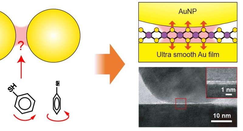
A research group led by Shunping Zhang and Hongxing Xu at Wuhan University, China, has developed a quantitative SERS technique to probe the maximum plasmonic fields before effects such as electron tunneling become dominant. The researchers turned to molybdenum disulfide (MoS2) — a graphene-like, two-dimensional atomic layer to tune the distance between a gold nanoparticle and a smooth gold film.
Plasmonic field enhancement is the cornerstone of a wide range of applications including surface enhanced spectroscopy, sensing, nonlinear optics, and light harvesting. The most intense plasmonic fields usually appear within narrow gaps between adjacent metallic nanostructures, especially when the separation goes down to subnanometer scale. However, experimentally probing the plasmonic fields in such a tiny volume still challenges the nanofabrication and detection techniques.
Measuring surface-enhanced Raman scattering (SERS) signals from a probe inside the nanogap region is a promising avenue to do that, but the method still faces several intractable issues: (i) how to create a width-controllable subnanometer gap with well-defined geometry, (ii) how to insert the nanoprobe into such narrow gap, and more importantly, (iii) how to control the alignment of the probe with respect to the strongest plasmonic field component. What’s more, the excitation laser should match with the plasmonic resonances in both wavelength and polarization for the maximum plasmonic enhancement. These requirements are difficult to satisfy simultaneously in traditional SERS using molecules as probe.
To overcome all these limitations, a research group led by Shunping Zhang and Hongxing Xu at Wuhan University, China, has developed a quantitative SERS technique to probe the maximum plasmonic fields before effects such as electron tunneling become dominant. The researchers turned to molybdenum disulfide (MoS2), a graphene-like, two-dimensional atomic layer to tune the distance between a gold nanoparticle and a smooth gold film. For the first time, the plasmonic near-field components in vertical and horizontal directions within atom-thick plasmonic nanocavities were quantitatively measured by using tiny flakes of two-dimensional atomic crystals as probes.
Conventional SERS probes using molecule are hard to control while a 2D material is perfect probe to the plasmonic fields in a nanogap. Credit: Wen Chen, Shunping Zhang, Meng Kang, Weikang Liu, Zhenwei Ou, Yang Li, Yexin Zhang, Zhiqiang Guan, Hongxing Xu, Probing the limits of plasmonic enhancement using a two-dimensional atomic crystal probe, Light: Science and Applications, doi: 10.1038/s41377-018-0056-3
In their configuration, the researchers can ensure that the probe filled in the gap has a well-defined lattice orientation such that the lattice vibrations are precisely aligned with the plasmonic field components. These lattice probes are free of optical bleaching or molecule hopping (in/out of the hotspot) as in traditional SERS experiments. They achieved the quantitative extraction of plasmonic fields in the nanogap by measuring the SERS intensity from the out-of-plane and in-plane phonon modes of the MoS2.
The robustness of the 2-D atomic crystal as SERS probes promote SERS to be a quantitative analytic tool instead of a qualitative one in most previous applications. Also, these unique designs could provide an important guide for further understanding quantum mechanical effects as well as plasmon-enhanced photon-phonon interactions and promoting relevant new applications, such as quantum plasmonics and nanogap optomechanics.
Source: Changchun Institute of Optics, Fine Mechanics and Physics