Imperfections in the regular atomic arrangements in crystals determine many of the properties of a material, and their diffusion is behind many microstructural changes in solids. However, imaging non-repeating atomic arrangements is difficult in conventional materials. Now, researchers at the University of Vienna have directly imaged the diffusion of a butterfly-shaped atomic defect in graphene, the recently discovered two-dimensional wonder material, over long image sequences. The results are published in the journal Nature Communications.
Atomic scale defects are always present in materials. For conventional materials they are hidden inside a large number of perfectly arranged atoms, except for at the surface. However, the situation is different in the case of low-dimensional materials like graphene.
Graphene is a honeycomb-like arrangement of carbon atoms only one carbon atom thick. Since its discovery in 2004, several remarkable properties of this material have been measured. For example, it is stronger than diamond and conducts electricity better than copper, but is nevertheless transparent and remarkably flexible. Because all of the atoms in graphene are at the surface, individual atoms and any defects in the structure are directly visible in a high resolution electron microscope, but at the same time they easily interact with the environment.
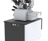
The defect the researchers concentrated on in the recent study in Vienna is a double vacancy that forms when two atoms are missing from the crystal. In the most stable form of this defect the hexagons of the graphene lattice transform into an arrangement of four pentagons and four heptagons (five and seven-membered carbon rings, respectively) which looks like an atomic-scale butterfly. The study was carried out with the Nion UltraSTEM 100 microscope, which was installed in Vienna only last year. The combination of ultra high vacuum and low acceleration voltage of this device were key components for the success of the study. In earlier experiments, the defects have always rapidly evolved into more complex structures or converted back into crystalline graphene, thus preventing the continuous imaging of their diffusion over long periods of time. Now, the defects remained stable for a longer amount of time that allowed a statistical analysis of their motion.
The researchers used the electron beam of the microscope to transform the defect between different arrangements, which resulted in a migration of the structure from one image to the next. “It was remarkable to see for the first time how a defect transforms and migrates in the crystal over several minutes while we are watching it,” says Dr. Jani Kotakoski, the lead author of the study. A careful analysis of the path of the defect revealed that the defect performed a random walk through the crystal.
“Our study opens a new route for the direct study of defect migration and diffusion in low-dimensional materials, which can also lead to new insights into defect dynamics in solids in general,” he concludes.
Source: University of Vienna