Over the last two decades, scientists have discovered that the optical microscope can be used to detect, track and image objects much smaller than their traditional limit — about half the wavelength of visible light, or a few hundred nanometers.
That pioneering research, which won the 2014 Nobel Prize in Chemistry, has enabled researchers to track proteins in fertilized eggs, visualize how molecules form electrical connections between nerve cells in the brain, and study the nanoscale motion of miniature motors.
Now, research developments at the National Institute of Standards and Technology (NIST) enable the microscopes to measure these nanometer-scale details with a new level of accuracy.
“We put the optical microscope under a microscope to achieve accuracy near the atomic scale,” says NIST’s Samuel Stavis, who served as the project leader for these efforts.
Because optical microscopes have not traditionally been used to study the nanometer scale, they typically lack the calibration — comparison to a standard to check that a result is correct — necessary to obtain information that is accurate at that scale. A microscope may be precise, consistently indicating the same position for a single molecule or nanoparticle. Yet, at the same time, it can be highly inaccurate—the location of the object identified by the microscope to within a billionth of a meter may, in fact, be millionths of a meter off due to unaccounted-for errors. “Precision without accuracy can be very misleading,” says Jon Geist, a NIST co-author of the study.
To address the problem, NIST has developed a new calibration process that closely examines and corrects these imaging errors. The process uses reference materials — objects with characteristics that are well-known and stable — that have the potential for mass production and widespread distribution to individual laboratories.
This is important because optical microscopes are common laboratory instruments that can easily magnify different samples, ranging from delicate biological specimens to electrical and mechanical devices. As well, optical microscopes are becoming increasingly capable and economical as they incorporate scientific versions of the lights and cameras in smartphones.
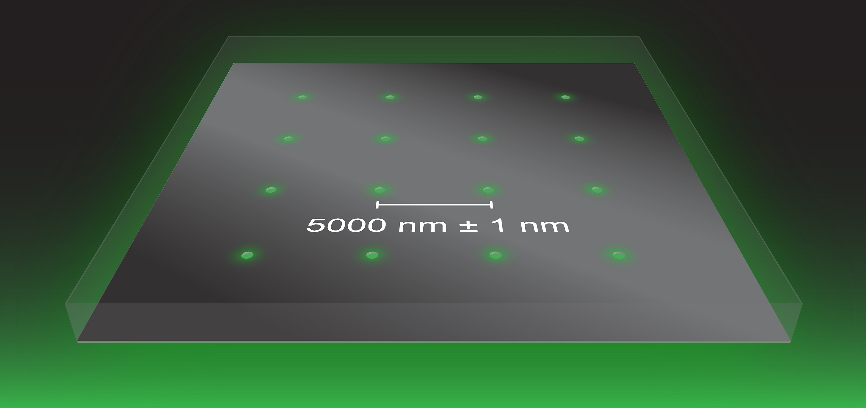
Illustration shows an array of apertures with a spacing of 5000 nanometers (nm) ± 1 nm. The apertures pass light through a metal film on a glass slide. Imaging the aperture array with an optical microscope results in apparent errors in the spacing between apertures. Knowledge of the true spacing allows correction of these imaging errors. This calibration process enables accurate measurements of position across a large image. Image: NIST
The NIST team relied on nanometer-scale fabrication processes to develop the reference material. The researchers used electron beams and ion milling to form an array of pinhole apertures through a thin film of platinum on a glass slide. The process enabled the team to space the apertures 5,000 nanometers apart, to within an accuracy of about 1 nanometer. In this way, the researchers built a measure of accuracy into the aperture positions.
Shining light through the array of apertures creates an array of points for imaging. But because all microscope lenses have imperfections, errors inevitably occur during imaging that change the apparent positions of the points, making the spacing between the apertures appear to be larger or smaller than the actual spacing engineered by the team. Knowledge of the true spacing allows correction of the imaging errors and calibration of the microscope for measurements of position with high accuracy across a wide field of view.
Even a small error can lead to a large problem. Consider, for example, a microscope having an actual magnification of 103 times when the expected magnification, as specified by the manufacturer, is 100 times. The resulting error of 3 percent adds up over large distances across a microscope image. Because of lens imperfections, a subtler problem also occurs — the microscope magnification changes across the image, causing image distortion. To solve this problem, the NIST team designed aperture arrays and calibration processes that worked across large fields of view.
The aperture arrays, which would enable individual researchers to perform calibrations in their own laboratories, could improve by a factor of 10,000 the ability of optical microscopes to accurately locate the position of single molecules and nanoparticles.
Stavis and his colleagues, including first author Craig Copeland of NIST and the Maryland NanoCenter at the University of Maryland, reported their findings in a recently posted article in Light: Science & Applications.
“We have identified and solved an underappreciated problem,” says Copeland.
Having calibrated their optical microscope using the arrays, the team reversed the process, using their microscope to identify imperfections in the prototype arrays from the nanofabrication process. “We tested the limits of nanofabrication to control the aperture spacing,” notes co-author Rob Ilic, manager of NIST’s NanoFab. The ease and speed of optical microscopy could facilitate quality control of aperture arrays in a production process.
Finally, the team exploited the inherent stability of the aperture arrays to evaluate whether fluorescent nanoparticles, often used as fixed points of reference in optical microscopy, actually remained fixed to a particular point or if they moved around. The researchers found that while unintentional motions of their optical microscope made views of the nanoparticles blurry, using the aperture array showed that the nanoparticles were not actually moving at atomic scales.
Source: NIST


