Research & Development World

  • R&D World Home
  • Topics
    • Aerospace
    • Automotive
    • Biotech
    • Careers
    • Chemistry
    • Environment
    • Energy
    • Life Science
    • Material Science
    • R&D Management
    • Physics
  • Technology
    • 3D Printing
    • A.I./Robotics
    • Software
    • Battery Technology
    • Controlled Environments
      • Cleanrooms
      • Graphene
      • Lasers
      • Regulations/Standards
      • Sensors
    • Imaging
    • Nanotechnology
    • Scientific Computing
      • Big Data
      • HPC/Supercomputing
      • Informatics
      • Security
    • Semiconductors
  • R&D Market Pulse
  • R&D 100
    • Call for Nominations: The 2025 R&D 100 Awards
    • R&D 100 Awards Event
    • R&D 100 Submissions
    • Winner Archive
    • Explore the 2024 R&D 100 award winners and finalists
  • Resources
    • Research Reports
    • Digital Issues
    • R&D Index
    • Subscribe
    • Video
    • Webinars
  • Global Funding Forecast
  • Top Labs
  • Advertise
  • SUBSCRIBE

Optical Nanoantennas Set Stage for NEMS Lab-on-a-Chip Revolution

By R&D Editors | February 25, 2015

Schematic representation of unidirectional cubic nanoantennas inducing directionality to omnidirectional nanoemitters (light sources, e.g., spasers, quantum dots), to precisely focus light with adjustable beam width and intensity, which can be tuned by adjusting the length of nanocube chain or intercube spacing. These ultra-narrow directional beams can play multiple roles in lab-on-a-chip devices such as illumination sources in microfluidic analysis or minute deflection registers in nanocantilever based sensors. All these signals are further detected in the photodetectors and get processed by on-chip signal processing circuitry for bio-molecular identification. CREDIT: D. Sikdar and M. Premaratne/Monash UniversityNewly developed tiny antennas, likened to spotlights on the nanoscale, offer the potential to measure food safety, identify pollutants in the air and even quickly diagnose and treat cancer, according to the Australian scientists who created them. The new antennas are cubic in shape. They do a better job than previous spherical ones at directing an ultra-narrow beam of light where it is needed, with little or no loss due to heating and scattering, they say.

In a paper published in the Journal of Applied Physics, from AIP Publishing, Debabrata Sikdar of Monash University in Victoria, Australia, and colleagues describe these and other envisioned applications for their nanocubes in “laboratories-on-a-chip.” The cubes, composed of insulating, rather than conducting or semiconducting materials as were the spherical versions, are easier to fabricate as well as more effective, he says.

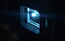
Sikdar’s paper presents analysis and simulation of 200-nanometer dielectric (nonconductive) nanoncubes placed in the path of visible and near-infrared light sources. The nanocubes are arranged in a chain, and the space between them can be adjusted to fine-tune the light beam as needed for various applications. As the separation between cubes increases, the angular width of the beam narrows and directionality improves, the researchers say.

“Unidirectional nanoantennas induce directionality to any omnidirectional light emitters like microlasers, nanolasers or spasers, and even quantum dots,” Sikdar said in an interview. Spasers are similar to lasers, but employ minute oscillations of electrons rather than light. Quantum dots are tiny crystals that produce specific colors, based on their size, and are widely used in color televisions. “Analogous to nanoscale spotlights, the cubic antennas focus light with precise control over direction and beam width,” he said.

The new cubic nanoantennas have the potential to revolutionize the infant field of nano-electromechanical systems (NEMS). “These unidirectional nanoantennas are most suitable for integrated optics-based biosensors to detect proteins, DNA, antibodies, enzymes, etc., in truly portable lab-on-a-chip platforms of the future,” Sikdar says. “They can also potentially replace the lossy on-chip IC (integrated circuit) interconnects, via transmitting optical signals within and among ICs, to ensure ultrafast data processing while minimizing device heating,” he adds.

Sikdar and his colleagues plan to begin constructing unidirectional cubic NEMS antennas in the near future at the Melbourne Center for Nanofabrication. “We would like to collaborate with other research groups across the world, making all these wonders possible,” he says.

Release Date: February 24, 2015
Source: American Institute of Physics


Related Articles Read More >

Illustration of ultracold atoms (gold) flowing frictionlessly along a laser boundary (green), representing the quantum phenomenon of edge states.
MIT physicists directly observe frictionless ‘edge state’ flow in ultracold atoms, offering a glimpse of super-efficient electronics
NTT Research scientist in cleanroom suit working on advanced photonic equipment
NTT Research bets light-based computing can tackles AI’s energy crisis
Scientists claim to generate world’s strongest terahertz radiation
SLAC fires up the world’s most powerful X-ray laser: LCLS-II ushers in a new era of science
rd newsletter
EXPAND YOUR KNOWLEDGE AND STAY CONNECTED
Get the latest info on technologies, trends, and strategies in Research & Development.
RD 25 Power Index

R&D World Digital Issues

Fall 2024 issue

Browse the most current issue of R&D World and back issues in an easy to use high quality format. Clip, share and download with the leading R&D magazine today.

Research & Development World
  • Subscribe to R&D World Magazine
  • Enews Sign Up
  • Contact Us
  • About Us
  • Drug Discovery & Development
  • Pharmaceutical Processing
  • Global Funding Forecast

Copyright © 2025 WTWH Media LLC. All Rights Reserved. The material on this site may not be reproduced, distributed, transmitted, cached or otherwise used, except with the prior written permission of WTWH Media
Privacy Policy | Advertising | About Us

Search R&D World

  • R&D World Home
  • Topics
    • Aerospace
    • Automotive
    • Biotech
    • Careers
    • Chemistry
    • Environment
    • Energy
    • Life Science
    • Material Science
    • R&D Management
    • Physics
  • Technology
    • 3D Printing
    • A.I./Robotics
    • Software
    • Battery Technology
    • Controlled Environments
      • Cleanrooms
      • Graphene
      • Lasers
      • Regulations/Standards
      • Sensors
    • Imaging
    • Nanotechnology
    • Scientific Computing
      • Big Data
      • HPC/Supercomputing
      • Informatics
      • Security
    • Semiconductors
  • R&D Market Pulse
  • R&D 100
    • Call for Nominations: The 2025 R&D 100 Awards
    • R&D 100 Awards Event
    • R&D 100 Submissions
    • Winner Archive
    • Explore the 2024 R&D 100 award winners and finalists
  • Resources
    • Research Reports
    • Digital Issues
    • R&D Index
    • Subscribe
    • Video
    • Webinars
  • Global Funding Forecast
  • Top Labs
  • Advertise
  • SUBSCRIBE