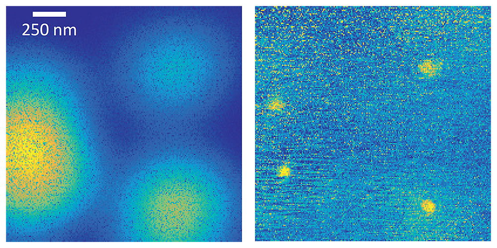
Image of quantum dots in a semiconductor: whereas the image taken with a normal microscope is blurry (left), the new method (right) clearly shows four quantum dots (bright yellow spots). Image: University of Basel, Department of Physics
Physicists have developed a technique based on optical microscopy that can be used to create images of atoms on the nanoscale. In particular, the new method allows the imaging of quantum dots in a semiconductor chip. Together with colleagues from the University of Bochum, scientists from the University of Basel’s Department of Physics and the Swiss Nanoscience Institute reported the findings in the journal Nature Photonics.
Microscopes allow us to see structures that are otherwise invisible to the human eye. However, conventional optical microscopes cannot be used to image individual molecules and atoms, which measure just fractions of a nanometer across. This has to do with the wave nature of light and the associated laws of physics, which were formulated by the German physicist Ernst Abbe back in 1873.
According to these laws, a microscope’s maximum resolution is equal to half the wavelength of the light used. For example, if you use green light with a wavelength of 500 nanometers, an optical microscope can, at best, distinguish objects at a distance of 250 nanometers.
In recent years, however, scientists have managed to get around this resolution limit and generate images of structures measuring just a few nanometers across. To do so, they used lasers of various wavelengths to trigger fluorescence in molecules in part of the substance while suppressing it in the surrounding areas. This allows them to image structures such as dye molecules, which are just a few nanometers in size. The development of this method (Stimulated Emission Depletion, STED) was honored with the Nobel Prize in Chemistry 2014.
Timo Kaldewey, from Professor Richard Warburton’s team at the University of Basel’s Department of Physics and Swiss Nanoscience Institute, has now worked with colleagues at Ruhr-University Bochum (Germany) to develop a similar technique that allows the imaging of nanoscale objects, particularly a quantum mechanical two-level system.
The physicists studied what are known as quantum dots, artificial atoms in a semiconductor, which the new method was able to image as bright spots. The scientists excited the atoms with a pulsed laser, which changes its color during each pulse. As a result, the atom’s fluorescence is switched on and off.
Whereas the STED method only works by occupying at least four different energy levels in response to the laser excitation, the new method from Basel also works with atoms that have just two energy states. Two-state systems of this kind constitute important model systems for quantum mechanics.
Unlike STED microscopy, the new method also releases no heat. “This is a huge advantage, as any heat released can destroy the molecules you’re examining,” explains Warburton. “Our nanoscope is suitable for all objects with two energy levels, such as real atoms, cold molecules, quantum dots, or color centers.”
The project received funding from, among other sources, the National Center of Competence in Research “Quantum Science and Technology” (NCCR QSIT), the Swiss National Science Foundation, and the European Union under the FP7 program.
Source: University of Basel


