Research & Development World

  • R&D World Home
  • Topics
    • Aerospace
    • Automotive
    • Biotech
    • Careers
    • Chemistry
    • Environment
    • Energy
    • Life Science
    • Material Science
    • R&D Management
    • Physics
  • Technology
    • 3D Printing
    • A.I./Robotics
    • Software
    • Battery Technology
    • Controlled Environments
      • Cleanrooms
      • Graphene
      • Lasers
      • Regulations/Standards
      • Sensors
    • Imaging
    • Nanotechnology
    • Scientific Computing
      • Big Data
      • HPC/Supercomputing
      • Informatics
      • Security
    • Semiconductors
  • R&D Market Pulse
  • R&D 100
    • Call for Nominations: The 2025 R&D 100 Awards
    • R&D 100 Awards Event
    • R&D 100 Submissions
    • Winner Archive
    • Explore the 2024 R&D 100 award winners and finalists
  • Resources
    • Research Reports
    • Digital Issues
    • R&D Index
    • Subscribe
    • Video
    • Webinars
  • Global Funding Forecast
  • Top Labs
  • Advertise
  • SUBSCRIBE

Plasma—Cleaning and Activation

By R&D Editors | April 18, 2011

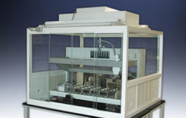
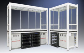
Plasma, a gaseous mixture of atoms, molecules, ions, and free electrons, allows for efficient surface treatment of electronic components and parts made of different materials.

In this, organic contaminations such as oils and greases are cleaned and simultaneously the surface is activated. This double function is based on a physical and chemical reaction of the procedure. Depending on the application case, low pressure plasmas or inline-compatible atmospheric pressure plasmas are used. Using the former, it is possible to implement both oxidizing and reducing processes. Within the oxidizing plasma, organic contaminations such as greases, oils, and adhesive residua can be removed before soldering or bonding. Reducing plasma processes are mainly used to optimize bond connections by means of reducing galvanically applied metal layers. In the electronics industry, processes of surface cleaning and activation by means of atmospheric pressure plasmas are used before printing, before gluing, or before pouring electronic printed circuit boards and semiconductors, in the field of optoelectronic component production, as well as before wire bonding. A joint project also deals with barrier coatings by means of inline-compatible atmospheric pressure plasmas for selective ageing and corrosion protection of electronic components.

From: Cleaning Strategies for Electronics Production

Related Articles Read More >

6 essentials for seismic rated cleanrooms
Critical Spaces Control Platform
Phoenix Critical Spaces Control Platform uses automation to direct airflow
Endiatx
Endiatx aims to boldly go beyond traditional endoscopy and, eventually, redefine surgical scale
FMN Laboratory researcher in a cleanroom
Take our quiz to test your cleanroom IQ, covering everything from ISO Classes to ULPA filtration
rd newsletter
EXPAND YOUR KNOWLEDGE AND STAY CONNECTED
Get the latest info on technologies, trends, and strategies in Research & Development.
RD 25 Power Index

R&D World Digital Issues

Fall 2024 issue

Browse the most current issue of R&D World and back issues in an easy to use high quality format. Clip, share and download with the leading R&D magazine today.

Research & Development World
  • Subscribe to R&D World Magazine
  • Enews Sign Up
  • Contact Us
  • About Us
  • Drug Discovery & Development
  • Pharmaceutical Processing
  • Global Funding Forecast

Copyright © 2025 WTWH Media LLC. All Rights Reserved. The material on this site may not be reproduced, distributed, transmitted, cached or otherwise used, except with the prior written permission of WTWH Media
Privacy Policy | Advertising | About Us

Search R&D World

  • R&D World Home
  • Topics
    • Aerospace
    • Automotive
    • Biotech
    • Careers
    • Chemistry
    • Environment
    • Energy
    • Life Science
    • Material Science
    • R&D Management
    • Physics
  • Technology
    • 3D Printing
    • A.I./Robotics
    • Software
    • Battery Technology
    • Controlled Environments
      • Cleanrooms
      • Graphene
      • Lasers
      • Regulations/Standards
      • Sensors
    • Imaging
    • Nanotechnology
    • Scientific Computing
      • Big Data
      • HPC/Supercomputing
      • Informatics
      • Security
    • Semiconductors
  • R&D Market Pulse
  • R&D 100
    • Call for Nominations: The 2025 R&D 100 Awards
    • R&D 100 Awards Event
    • R&D 100 Submissions
    • Winner Archive
    • Explore the 2024 R&D 100 award winners and finalists
  • Resources
    • Research Reports
    • Digital Issues
    • R&D Index
    • Subscribe
    • Video
    • Webinars
  • Global Funding Forecast
  • Top Labs
  • Advertise
  • SUBSCRIBE