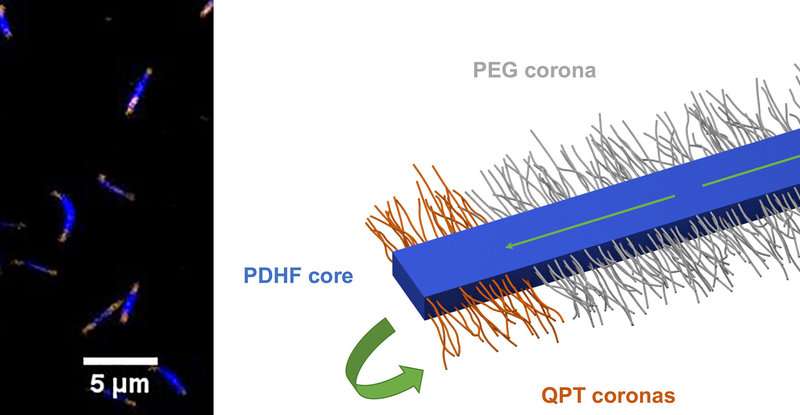
Image showing light emission from the polymeric nanostructures and schematic of a single nanostructure. Credit: University of Bristol
Scientists from the universities of Bristol and Cambridge have found a way to create polymeric semiconductor nanostructures that absorb light and transport its energy further than previously observed.
This could pave the way for more flexible and more efficient solar cells and photodetectors.
The researchers, whose work appears in the journal Science, say their findings could be a “game changer” by allowing the energy from sunlight absorbed in these materials to be captured and used more efficiently.
Lightweight semiconducting plastics are now widely used in mass market electronic displays such those found in phones, tablets and flat screen televisions. However, using these materials to convert sunlight into electricity, to make solar cells, is far more complex.
The photo-excited states—which is when photons of light are absorbed by the semiconducting material—need to move so that they can be “harvested” before they lose their energy in less useful ways. These excitations typically only travel ca. 10 nanometres in polymeric semiconductors, thus requiring the construction of structures patterned on this length-scale to maximise the “harvest”.
In the chemistry labs of the University of Bristol, Dr. Xu-Hui Jin and colleagues developed a novel way to make highly ordered crystalline semiconducting structures using polymers.
While in the Cavendish Laboratory in Cambridge, Dr. Michael Price measured the distance that the photo-exited states can travel, which reached distances of 200 nanometres—20 times further than was previously possible.
200 nanometres is especially significant because it is greater than the thickness of material needed to completely absorb ambient light thus making these polymers more suitable as “light harvesters” for solar cells and photodetectors.
Dr. George Whittell from Bristol’s School of Chemistry, explains: “The gain in efficiency would actually be for two reasons: first, because the energetic particles travel further, they are easier to “harvest”, and second, we could now incorporate layers ca. 100 nanometres thick, which is the minimum thickness needed to absorb all the energy from light—the so-called optical absorption depth. Previously, in layers this thick, the particles were unable to travel far enough to reach the surfaces.”
Co-researcher Professor Richard Friend, from Cambridge, added: “The distance that energy can be moved in these materials comes as a big surprise and points to the role of unexpected quantum coherent transport processes.”
The research team now plans to prepare structures thicker than those in the current study and greater than the optical absorption depth, with a view to building prototype solar cells based on this technology.
They are also preparing other structures capable of using light to perform chemical reactions, such as the splitting of water into hydrogen and oxygen.


