Research & Development World

  • R&D World Home
  • Topics
    • Aerospace
    • Automotive
    • Biotech
    • Careers
    • Chemistry
    • Environment
    • Energy
    • Life Science
    • Material Science
    • R&D Management
    • Physics
  • Technology
    • 3D Printing
    • A.I./Robotics
    • Software
    • Battery Technology
    • Controlled Environments
      • Cleanrooms
      • Graphene
      • Lasers
      • Regulations/Standards
      • Sensors
    • Imaging
    • Nanotechnology
    • Scientific Computing
      • Big Data
      • HPC/Supercomputing
      • Informatics
      • Security
    • Semiconductors
  • R&D Market Pulse
  • R&D 100
    • Call for Nominations: The 2025 R&D 100 Awards
    • R&D 100 Awards Event
    • R&D 100 Submissions
    • Winner Archive
    • Explore the 2024 R&D 100 award winners and finalists
  • Resources
    • Research Reports
    • Digital Issues
    • R&D Index
    • Subscribe
    • Video
    • Webinars
  • Global Funding Forecast
  • Top Labs
  • Advertise
  • SUBSCRIBE

Scientists Untangle Nanotubes to Release Electronics Potential

By R&D Editors | October 21, 2013

A multiwall carbon nanotube sample. (Source: Wikimedia/Kristian Molhave)Researchers have demonstrated how to produce electronic inks for the development of new applications using the ‘wonder material,’ carbon nanotubes.

Carbon nanotubes are lightweight, strong and conduct electricity, which make them ideal components in new electronics devices, such as tablet computers and touchscreen phones, but cannot be used without being separated out from their natural tangled state.

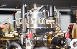
In the video (link above), Dr Stephen Hodge and Professor Milo Shaffer, both from Imperial’s Department of Chemistry, talk about the challenges of unravelling and applying carbon nanotubes in the laboratory and how the method is being scaled up to meet the requirements of industrial-scale manufacturing.

Carbon nanotubes are hollow, spaghetti-like strands made from the same material as graphene; only one nanometre thick but with theoretically unlimited length. This ‘wonder material’ shares many of graphene’s properties, and has attracted much public and private investment into making it into useful technology.

By giving the nanotubes an electrical charge, they were able to pull apart individual strands. Using this method, nanotubes can be sorted or refined, then deposited in a uniform layer onto the surface of any object.

Working with an industrial partner, Linde Electronics, they have produced an electrically-conductive carbon nanotube ink, which coats carbon nanotubes onto ultra-thin sheets of transparent film that are used to manufacture flat-screen televisions and computer screens.

This was developed by Professor Shaffer and colleagues from the London Centre for Nanotechnology, which includes fellow Imperial scientist Dr. Siân Fogden, as well as Dr. Chris Howard and Professor Neal Skipper from UCL.

The research is written up in the journals Nature Communications and ACS Nano.

Related Articles Read More >

Berkeley Lab’s Dell and NVIDIA-powered ‘Doudna’ supercomputer to enable real-time data access for 11,000 researchers
QED-C outlines road map for merging quantum and AI
Quantum computing hardware advance slashes superinductor capacitance >60%, cutting substrate loss
Hold your exaflops! Why comparing AI clusters to supercomputers is bananas
rd newsletter
EXPAND YOUR KNOWLEDGE AND STAY CONNECTED
Get the latest info on technologies, trends, and strategies in Research & Development.
RD 25 Power Index

R&D World Digital Issues

Fall 2024 issue

Browse the most current issue of R&D World and back issues in an easy to use high quality format. Clip, share and download with the leading R&D magazine today.

Research & Development World
  • Subscribe to R&D World Magazine
  • Enews Sign Up
  • Contact Us
  • About Us
  • Drug Discovery & Development
  • Pharmaceutical Processing
  • Global Funding Forecast

Copyright © 2025 WTWH Media LLC. All Rights Reserved. The material on this site may not be reproduced, distributed, transmitted, cached or otherwise used, except with the prior written permission of WTWH Media
Privacy Policy | Advertising | About Us

Search R&D World

  • R&D World Home
  • Topics
    • Aerospace
    • Automotive
    • Biotech
    • Careers
    • Chemistry
    • Environment
    • Energy
    • Life Science
    • Material Science
    • R&D Management
    • Physics
  • Technology
    • 3D Printing
    • A.I./Robotics
    • Software
    • Battery Technology
    • Controlled Environments
      • Cleanrooms
      • Graphene
      • Lasers
      • Regulations/Standards
      • Sensors
    • Imaging
    • Nanotechnology
    • Scientific Computing
      • Big Data
      • HPC/Supercomputing
      • Informatics
      • Security
    • Semiconductors
  • R&D Market Pulse
  • R&D 100
    • Call for Nominations: The 2025 R&D 100 Awards
    • R&D 100 Awards Event
    • R&D 100 Submissions
    • Winner Archive
    • Explore the 2024 R&D 100 award winners and finalists
  • Resources
    • Research Reports
    • Digital Issues
    • R&D Index
    • Subscribe
    • Video
    • Webinars
  • Global Funding Forecast
  • Top Labs
  • Advertise
  • SUBSCRIBE