An international team of scientist of Peter the Great St. Petersburg Polytechnic University (SPbPU), Leibniz University Hannover (Leibniz Universität Hannover) and the Ioffe Institute report a way to improve nanocomposite material, opening new opportunities in industry. The study, titled “The mechanism of charge carrier generation at the TiO2 — n-Si heterojunction activated by gold nanoparticles,” is published in Semiconductor Science and Technology.
The study is dedicated to a composite semiconductor based on titanium dioxide. Its applications are widely studied by researchers all over the world. But the processes that take place in this material are very complex. Therefore, to use the semiconductor more effectively, it is necessary to ensure that the energy enclosed between its layers can be released and transmitted.
In the framework of the experiments, the researchers propose a qualitative model to explain the complex processes. They used a composite material consisting of a silicon wafer (standard silicon wafer used in electronic devices), gold nanoparticles and a thin layer of titanium dioxide. During the experiment to transfer the energy inside the material, the researchers intended to isolate nanoparticles from silicon. If nanoparticles are not isolated from the silicon wafer, then the energy can’t be transmitted to the silicon nor to the titanium dioxide, leading to energy loss.
“The obtained material was a silicon wafer with pillar-like structures grown on its surface. It was used as a substrate for the sample. Gold nanoparticles were situated on top of these pillars and the whole structure was coated with titanium oxide. Thus, nanoparticles contacted only titanium dioxide, and simultaneously were isolated from silicon. The number of boundaries between the layers decreased, and we tried to describe the processes in the material. In addition, we assumed that this structure would increase the efficiency of using the energy of light illuminating the surface of our material,” says Dr. Maxim Mishin, professor of Physics, Chemistry, and Technology of Microsystems Equipment Department of SPbPU.
In St. Petersburg, an international scientific group established a model of a new structure, then the main part of the structure was created in Hannover: a silicon wafer with pillars and gold nanoparticles situated on top of it.
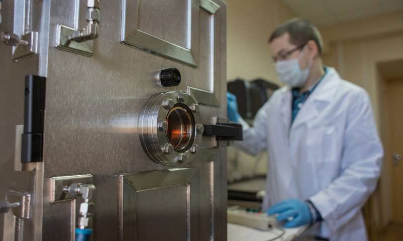
The international scientific group conducted the experiment with semiconductor based on titanium dioxide. Image: Peter the Great St.Petersburg Polytechnic University
The experiment was performed as follows. First, the wafer was oxidized, i.e., it was covered with a layer of the substrate, and gold nanoparticles were put on top of it. “After that, we faced the next task: to create pillars and to perform the etching of the substrate so that it is remained under the particles and not and in between them. Considering that we are dealing with the nanoscale—the diameter of gold nanoparticles is about 10 nanometers, and the height of the pillar is 80 nanometers—this is not a trivial task. The development of modern nanoelectronics makes it possible to use the so-called ‘dry’ etching methods such as reactive ion etching,” adds Dr. Marc Christopher Wurz from the Institute of Micro Production Technology at Leibniz University Hannover.
According to scientists, the process was not rapid. At the first stages of the experiment, while using the ion etching, all gold nanoparticles were simply demolished from the oxidized wafer. In the course of one week, the researchers were selecting the parameters for etching plasma system, so that the gold nanoparticles remained on the surface. The whole experiment was conducted within 10 days.
This scientific project is ongoing. The researchers report that this nanocomposite material can be used in optical devices operating in the visible light spectrum. In addition, it can be used as a catalyst to produce hydrogen from water, or to purify water by stimulating the decomposition of complex molecules. In addition, this material may be useful as an element of a sensor that detects gas leaks or increased concentration of harmful substances in the air.
Source: Peter the Great Saint-Petersburg Polytechnic University


