Research & Development World

  • R&D World Home
  • Topics
    • Aerospace
    • Automotive
    • Biotech
    • Careers
    • Chemistry
    • Environment
    • Energy
    • Life Science
    • Material Science
    • R&D Management
    • Physics
  • Technology
    • 3D Printing
    • A.I./Robotics
    • Software
    • Battery Technology
    • Controlled Environments
      • Cleanrooms
      • Graphene
      • Lasers
      • Regulations/Standards
      • Sensors
    • Imaging
    • Nanotechnology
    • Scientific Computing
      • Big Data
      • HPC/Supercomputing
      • Informatics
      • Security
    • Semiconductors
  • R&D Market Pulse
  • R&D 100
    • 2025 R&D 100 Award Winners
    • 2025 Professional Award Winners
    • 2025 Special Recognition Winners
    • R&D 100 Awards Event
    • R&D 100 Submissions
    • Winner Archive
  • Resources
    • Research Reports
    • Digital Issues
    • Educational Assets
    • R&D Index
    • Subscribe
    • Video
    • Webinars
    • Content submission guidelines for R&D World
  • Global Funding Forecast
  • Top Labs
  • Advertise
  • SUBSCRIBE

Semiconductors Have an Aligned Interface

By R&D Editors | November 13, 2017

Knowledge of the bandgap and band alignment of aluminum-nitride-based semiconductors is key to designing energy-efficient optical and power devices. © 2017 KAUST

The electronic characteristics of an interface between two wide bandgap semiconductors are determined by researchers at King Abdullah University of Science and Technology (KAUST): an insight that will help improve the efficiency of light-emitting and high-power electronic devices.

Semiconductors, such as silicon and gallium nitride, have electrical properties somewhere in between those of a conductor and an insulator. They only allow current to flow when electrons have enough energy to overcome a barrier known as bandgap. The bandgap — which may be direct or indirect, narrow or large — determines the properties of semiconductors and their consequent applications.

Materials with a large bandgap, for example, are useful in high-power electronics because they have larger breakdown voltage for energy-efficient transistors as compared with narrow bandgap materials, such as silicon. They can also produce light deep into the ultraviolet part of the spectrum, making them useful for disinfection and water purification.

These materials can be further tailored to a specific application by layering different semiconductors on top of each other to create a so-called heterostructure with the desired properties. But it is vital to understand how the bandgaps of two semiconductors align when semiconductors are brought together in this way.

Haiding Sun and principle investigator Xiaohang Li from KAUST and coworkers from the Georgia Institute of Technology report that they experimentally measured the alignment of two emerging large bandgap materials: boron aluminum nitride and aluminum gallium nitride.

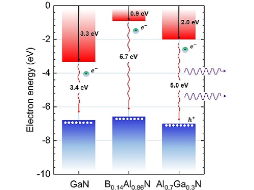
The 2014 Nobel Prize for physics was awarded in recognition of the development of gallium nitride light-emitting diodes. But, compared to gallium nitride, aluminum nitride has a much larger bandgap of 6.1 electronvolts. Its electronic properties can be tuned by replacing some of the aluminum atoms in the crystal with either boron or gallium.

The team created an interface between boron aluminum nitride with a boron to aluminum atom ratio of 14:86 and aluminum gallium nitride with a gallium nitride ratio of 30:70 on an aluminum-nitride-covered sapphire substrate.

They used high-resolution X-ray photoemission spectroscopy to measure the offset between the top and the bottom of the two material’s bandgaps. They show that the bandgaps have a staggered alignment, with both the top and bottom edge of the bandgap of the Al0.7Ga0.3N lower than the respective edge in B0.14Al0.86N.

“Based on the experimental results, we can achieve a much higher amount of two-dimensional electron gas sheet carrier concentration in such junction,” says Sun. “The determination of the band alignment of B0.14Al0.86N/Al0.7Ga0.3N heterojunction provides valuable support in the design of optical and electronic devices based on such junctions.”

Source: King Abdullah University of Science and Technology

Related Articles Read More >

CEA-Leti achieves 400°C CMOS fabrication milestone for 3D chip stacking
Materials driving the next phase in semiconductor performance
NVIDIA becomes major Intel CPU buyer in $5B collaboration
TOKYO, JAPAN - OCTOBER 2, 2016: Detail from Apple shop in Tokyo, Japan. Apple is American multinational corporation founded at 1976 at Cupertino, California.
iPhone 17 Pro, rumored to add vapor-chamber cooling and a 48MP telephoto, is tracking a September launch
rd newsletter
EXPAND YOUR KNOWLEDGE AND STAY CONNECTED
Get the latest info on technologies, trends, and strategies in Research & Development.
RD 25 Power Index

R&D World Digital Issues

Fall 2025 issue

Browse the most current issue of R&D World and back issues in an easy to use high quality format. Clip, share and download with the leading R&D magazine today.

R&D 100 Awards
Research & Development World
  • Subscribe to R&D World Magazine
  • Sign up for R&D World’s newsletter
  • Contact Us
  • About Us
  • Drug Discovery & Development
  • Pharmaceutical Processing
  • Global Funding Forecast

Copyright © 2026 WTWH Media LLC. All Rights Reserved. The material on this site may not be reproduced, distributed, transmitted, cached or otherwise used, except with the prior written permission of WTWH Media
Privacy Policy | Advertising | About Us

Search R&D World

  • R&D World Home
  • Topics
    • Aerospace
    • Automotive
    • Biotech
    • Careers
    • Chemistry
    • Environment
    • Energy
    • Life Science
    • Material Science
    • R&D Management
    • Physics
  • Technology
    • 3D Printing
    • A.I./Robotics
    • Software
    • Battery Technology
    • Controlled Environments
      • Cleanrooms
      • Graphene
      • Lasers
      • Regulations/Standards
      • Sensors
    • Imaging
    • Nanotechnology
    • Scientific Computing
      • Big Data
      • HPC/Supercomputing
      • Informatics
      • Security
    • Semiconductors
  • R&D Market Pulse
  • R&D 100
    • 2025 R&D 100 Award Winners
    • 2025 Professional Award Winners
    • 2025 Special Recognition Winners
    • R&D 100 Awards Event
    • R&D 100 Submissions
    • Winner Archive
  • Resources
    • Research Reports
    • Digital Issues
    • Educational Assets
    • R&D Index
    • Subscribe
    • Video
    • Webinars
    • Content submission guidelines for R&D World
  • Global Funding Forecast
  • Top Labs
  • Advertise
  • SUBSCRIBE