Research & Development World

  • R&D World Home
  • Topics
    • Aerospace
    • Automotive
    • Biotech
    • Careers
    • Chemistry
    • Environment
    • Energy
    • Life Science
    • Material Science
    • R&D Management
    • Physics
  • Technology
    • 3D Printing
    • A.I./Robotics
    • Software
    • Battery Technology
    • Controlled Environments
      • Cleanrooms
      • Graphene
      • Lasers
      • Regulations/Standards
      • Sensors
    • Imaging
    • Nanotechnology
    • Scientific Computing
      • Big Data
      • HPC/Supercomputing
      • Informatics
      • Security
    • Semiconductors
  • R&D Market Pulse
  • R&D 100
    • 2025 R&D 100 Award Winners
    • 2025 Professional Award Winners
    • 2025 Special Recognition Winners
    • R&D 100 Awards Event
    • R&D 100 Submissions
    • Winner Archive
  • Resources
    • Research Reports
    • Digital Issues
    • Educational Assets
    • R&D Index
    • Subscribe
    • Video
    • Webinars
    • Content submission guidelines for R&D World
  • Global Funding Forecast
  • Top Labs
  • Advertise
  • SUBSCRIBE

Silicon On Insulator Wafer Proves Useful for Microelectronics

By Aalto University | March 6, 2017

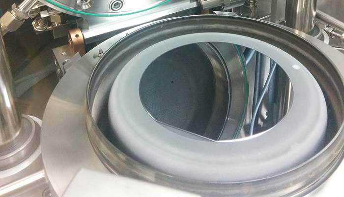
The researchers used Micronova’s cleanrooms and, in particular, a reactor designed for gallium nitride manufacturing. The image shows a six-inch substrate in the MOVPE reactor before manufacturing. Image: Aalto University/Jori Lemettinen

In cooperation with Okmetic Oy and the Polish ITME, researchers at Aalto University have studied the application of SOI (Silicon On Insulator) wafers, which are used as a platform for manufacturing different microelectronics components, as a substrate for producing gallium nitride crystals. The researchers compared the characteristics of gallium nitride (GaN) layers grown on SOI wafers to those grown on silicon substrates more commonly used for the process. In addition to high-performance silicon wafers, Okmetic also manufactures SOI wafers, in which a layer of silicon dioxide insulator is sandwiched between two silicon layers. The objective of the SOI technology is to improve the capacitive and insulating characteristics of the wafer.

“We used a standardized manufacturing process for comparing the wafer characteristics. GaN growth on SOI wafers produced a higher crystalline quality layer than on silicon wafers. In addition, the insulating layer in the SOI wafer improves breakdown characteristics, enabling the use of clearly higher voltages in power electronics. Similarly, in high frequency applications, the losses and crosstalk can be reduced,” explains Jori Lemettinen, a doctoral candidate from the Department of Electronics and Nanoengineering.

“GaN based components are becoming more common in power electronics and radio applications. The performance of GaN based devices can be improved by using a SOI wafer as the substrate,” adds Academy Research Fellow Sami Suihkonen.

Growth of GaN on a silicon substrate is challenging. GaN layers and devices can be grown on substrate material using metalorganic vapor phase epitaxy (MOVPE). When using silicon as a substrate the grown compound semiconductor materials have different coefficients of thermal expansion and lattice constants than a silicon wafer. These differences in their characteristics limit the crystalline quality that can be achieved and the maximum possible thickness of the produced layer.

“The research showed that the layered structure of an SOI wafer can act as a compliant substrate during gallium nitride layer growth and thus reduce defects and strain in the grown layers,” Lemettinen notes.

GaN based components are commonly used in blue and white LEDs. In power electronics applications, GaN diodes and transistors, in particular, have received interest, for example in frequency converters or electric cars. It is believed that in radio applications, 5G network base stations will use GaN based power amplifiers in the future. In electronics applications, a GaN transistor offers low resistance and enables high frequencies and power densities.

The article has been accepted for publication in the journal Semiconductor Science and Technology.

Source: Aalto University

Related Articles Read More >

Marktech expands large-area silicon photodiode portfolio for spectroscopy, medical diagnostics
R&D 100 Winner Spotlight: How Qnity beat the industry timeline on PFAS-free lithography
CEA-Leti achieves 400°C CMOS fabrication milestone for 3D chip stacking
Materials driving the next phase in semiconductor performance
rd newsletter
EXPAND YOUR KNOWLEDGE AND STAY CONNECTED
Get the latest info on technologies, trends, and strategies in Research & Development.
RD 25 Power Index

R&D World Digital Issues

Fall 2025 issue

Browse the most current issue of R&D World and back issues in an easy to use high quality format. Clip, share and download with the leading R&D magazine today.

R&D 100 Awards
Research & Development World
  • Subscribe to R&D World Magazine
  • Sign up for R&D World’s newsletter
  • Contact Us
  • About Us
  • Drug Discovery & Development
  • Pharmaceutical Processing
  • Global Funding Forecast

Copyright © 2026 WTWH Media LLC. All Rights Reserved. The material on this site may not be reproduced, distributed, transmitted, cached or otherwise used, except with the prior written permission of WTWH Media
Privacy Policy | Advertising | About Us

Search R&D World

  • R&D World Home
  • Topics
    • Aerospace
    • Automotive
    • Biotech
    • Careers
    • Chemistry
    • Environment
    • Energy
    • Life Science
    • Material Science
    • R&D Management
    • Physics
  • Technology
    • 3D Printing
    • A.I./Robotics
    • Software
    • Battery Technology
    • Controlled Environments
      • Cleanrooms
      • Graphene
      • Lasers
      • Regulations/Standards
      • Sensors
    • Imaging
    • Nanotechnology
    • Scientific Computing
      • Big Data
      • HPC/Supercomputing
      • Informatics
      • Security
    • Semiconductors
  • R&D Market Pulse
  • R&D 100
    • 2025 R&D 100 Award Winners
    • 2025 Professional Award Winners
    • 2025 Special Recognition Winners
    • R&D 100 Awards Event
    • R&D 100 Submissions
    • Winner Archive
  • Resources
    • Research Reports
    • Digital Issues
    • Educational Assets
    • R&D Index
    • Subscribe
    • Video
    • Webinars
    • Content submission guidelines for R&D World
  • Global Funding Forecast
  • Top Labs
  • Advertise
  • SUBSCRIBE