A new manufacturing technique uses a process similar to newspaper printing to form smoother and more flexible metals for making ultrafast electronic devices.
The low-cost process, developed by Purdue University researchers, combines tools already used in industry for manufacturing metals on a large scale, but uses the speed and precision of roll-to-roll newspaper printing to remove a couple of fabrication barriers in making electronics faster than they are today.
Cellphones, laptops, tablets, and many other electronics rely on their internal metallic circuits to process information at high speed. Current metal fabrication techniques tend to make these circuits by getting a thin rain of liquid metal drops to pass through a stencil mask in the shape of a circuit, kind of like spraying graffiti on walls.
“Unfortunately, this fabrication technique generates metallic circuits with rough surfaces, causing our electronic devices to heat up and drain their batteries faster,” says Ramses Martinez, assistant professor of industrial engineering and biomedical engineering.
Future ultrafast devices also will require much smaller metal components, which calls for a higher resolution to make them at these nanoscale sizes.
“Forming metals with increasingly smaller shapes requires molds with higher and higher definition, until you reach the nanoscale size,” Martinez says. “Adding the latest advances in nanotechnology requires us to pattern metals in sizes that are even smaller than the grains they are made of. It’s like making a sand castle smaller than a grain of sand.”
This so-called “formability limit” hampers the ability to manufacture materials with nanoscale resolution at high speed.
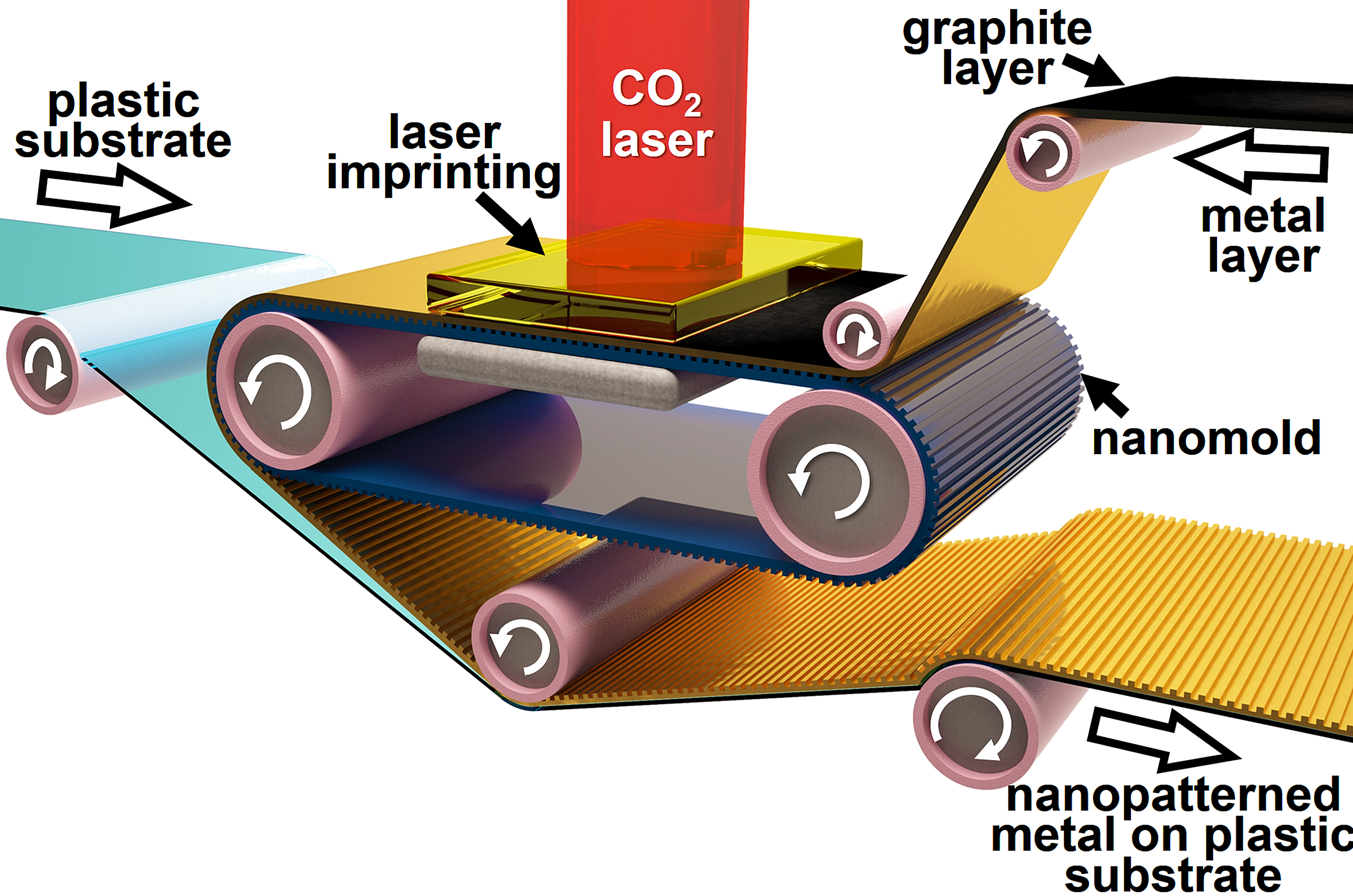
Roll-to-roll laser-induced superplasticity, a new fabrication method, prints metals at the nanoscale needed for making electronic devices ultrafast. Image: Purdue University/Ramses Martinez
Purdue researchers have addressed both of these issues — roughness and low resolution — with a new large-scale fabrication method that enables the forming of smooth metallic circuits at the nanoscale using conventional carbon dioxide lasers, which are already common for industrial cutting and engraving.
“Printing tiny metal components like newspapers makes them much smoother. This allows an electric current to travel better with less risk of overheating,” Martinez says.
The fabrication method, called roll-to-roll laser-induced superplasticity, uses a rolling stamp like the ones used to print newspapers at high speed. The technique can induce, for a brief period of time, “superelastic” behavior to different metals by applying high-energy laser shots, which enables the metal to flow into the nanoscale features of the rolling stamp — circumventing the formability limit.
“In the future, the roll-to-roll fabrication of devices using our technique could enable the creation of touch screens covered with nanostructures capable of interacting with light and generating 3D images, as well as the cost-effective fabrication of more sensitive biosensors,” Martinez says.
The researchers discuss their technology further in Nano Letters, an American Chemical Society publication. The work is financially supported by Purdue University; the Ross Fellowship program at Purdue; the Administrative Department of Science, Technology and Innovation of Colombia (Grant 567-2012); and Procter & Gamble (Grant 209621).
Source: Purdue University


