WEST LAFAYETTE, Ind. – Researchers have found a way to see synthetic nanostructures and molecules using a new type of super-resolution optical microscopy that does not require fluorescent dyes, representing a practical tool for biomedical and nanotechnology research.
“Super-resolution optical microscopy has opened a new window into the nanoscopic world,” said Ji-Xin Cheng, an associate professor of biomedical engineering and chemistry at Purdue University.
Conventional optical microscopes can resolve objects no smaller than about 300 nanometers, or billionths of a meter, a restriction known as the “diffraction limit,” which is defined as half the width of the wavelength of light being used to view the specimen. However, researchers want to view molecules such as proteins and lipids, as well as synthetic nanostructures like nanotubes, which are a few nanometers in diameter.
Such a capability could bring advances in a diverse range of disciplines, from medicine to nanoelectronics, Cheng said.
“The diffraction limit represents the fundamental limit of optical imaging resolution,” Cheng said. “Stefan Hell at the Max Planck Institute and others have developed super-resolution imaging methods that require fluorescent labels. Here, we demonstrate a new scheme for breaking the diffraction limit in optical imaging of non-fluorescent species. Because it is label-free, the signal is directly from the object so that we can learn more about the nanostructure.”
Findings are detailed in a research paper that appeared online April 28, 2013, in the journal Nature Photonics.
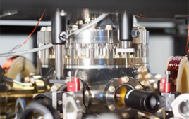
The imaging system, called saturated transient absorption microscopy, or STAM, uses a trio of laser beams, including a doughnut-shaped laser beam that selectively illuminates some molecules but not others. Electrons in the atoms of illuminated molecules are kicked temporarily into a higher energy level and are said to be excited, while the others remain in their “ground state.” Images are generated using a laser called a probe to compare the contrast between the excited and ground-state molecules.
The researchers demonstrated the technique, taking images of graphite “nanoplatelets” about 100 nanometers wide.
“It’s a proof of concept and has great potential for the study of nanomaterials, both natural and synthetic,” Cheng said.
The doughnut-shaped laser excitation technique, invented by researcher Stefan Hell, makes it possible to focus on yet smaller objects. Researchers hope to improve the imaging system to see objects about 10 nanometers in diameter, or about 30 times smaller than possible using conventional optical microscopes.
“We are not there yet, but a few schemes can be applied to further increase the resolution of our system,” Cheng said.
The paper was co-authored by biomedical engineering doctoral student Pu Wang; research scientist Mikhail N. Slipchenko; mechanical engineering doctoral student James Mitchell; Chen Yang, an assistant professor of physical chemistry at Purdue; Eric O. Potma, an associate professor of chemistry at the University of California, Irvine; Xianfan Xu, Purdue’s James J. and Carol L. Shuttleworth Professor of Mechanical Engineering; and Cheng.
Future research may include work to use lasers with shorter wavelengths of light. Because the wavelengths are shorter, the doughnut hole is smaller, possibly allowing researchers to focus on smaller objects.
The work will be discussed during the third annual Spectroscopic Imaging: A New Window into the Unseen World workshop on May 23 and 24 at Purdue. The workshop is hosted by the university’s Weldon School of Biomedical Engineering. More workshop information is available at http://www.conf.purdue.edu/cheng
The research is funded by the National Institutes of Health, National Science Foundation and the Defense Advanced Research Projects Agency.
ABSTRACT
Far-Field Imaging of Non-Fluorescent Species with Sub-Diffraction Resolution
Pu Wang1, #, Mikhail N. Slipchenko1, #, James Mitchell2, Chen Yang3, Eric O. Potma4, Xianfan Xu2, Ji-Xin Cheng13, *4
1 Weldon School of Biomedical Engineering, Purdue University
2 School of Mechanical Engineering and Birck Nanotechnology Center, Purdue University
3 Department of Chemistry, Purdue University
4 Department of Chemistry, University of California, Irvine
Super-resolution optical microscopy is opening a new window to unveil the unseen details on the nanoscopic scale. Current far-field super-resolution techniques rely on fluorescence as the read-out. Here, we demonstrate a scheme for breaking the diffraction limit in far-field imaging of non-fluorescent species by using spatially controlled saturation of electronic absorption. Our method is based on a pump-probe process where a modulated pump field perturbs the charge-carrier density in a sample, thus modulating the transmission of a probe field. A doughnut shape laser beam is then added to transiently saturate the electronic transition in the periphery of the focal volume, thus the induced modulation in the sequential probe pulse only occurs at the focal center. By raster scanning the three collinearly aligned beams, high-speed sub-diffraction-limited imaging of graphite nano-platelets was performed. This technique potentially enables super-resolution imaging of nano-materials and non-fluorescent chromophores, which may remain out of reach for fluorescence-based methods.