Research & Development World

  • R&D World Home
  • Topics
    • Aerospace
    • Automotive
    • Biotech
    • Careers
    • Chemistry
    • Environment
    • Energy
    • Life Science
    • Material Science
    • R&D Management
    • Physics
  • Technology
    • 3D Printing
    • A.I./Robotics
    • Software
    • Battery Technology
    • Controlled Environments
      • Cleanrooms
      • Graphene
      • Lasers
      • Regulations/Standards
      • Sensors
    • Imaging
    • Nanotechnology
    • Scientific Computing
      • Big Data
      • HPC/Supercomputing
      • Informatics
      • Security
    • Semiconductors
  • R&D Market Pulse
  • R&D 100
    • Call for Nominations: The 2025 R&D 100 Awards
    • R&D 100 Awards Event
    • R&D 100 Submissions
    • Winner Archive
    • Explore the 2024 R&D 100 award winners and finalists
  • Resources
    • Research Reports
    • Digital Issues
    • R&D Index
    • Subscribe
    • Video
    • Webinars
  • Global Funding Forecast
  • Top Labs
  • Advertise
  • SUBSCRIBE

Think Small

By R&D Editors | January 28, 2009

To meet cleanliness specifications, the first thought is frequently “Build it in a Cleanroom.” However, not every critical component need be processed in a large, tightly specified cleanroom by gowned personnel.

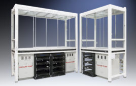
Sometimes mini-environments provide a superior and cost-effective option. We are expanding the concept of the mini-environment from that often used in microelectronics to encompass any small, atmosphere-controlled enclosure that allows processing without contaminating the product or the external environment.

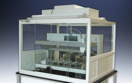
While most processing is done in large air and humidity-controlled cleanrooms, critical processing of wafers is frequently performed in smaller self-contained enclosures that contain the wafers and robotically-operated processing tools. The super-critical cleanliness environments required for processing or transport are confined to small volumes, providing cleanliness levels unachievable even with head-to-foot gowning of personnel.

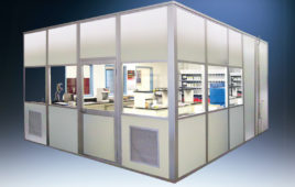
A mini-environment approach to cleaning critical components can be employed even when required cleanliness levels are not so severe as for semiconductor wafer processing. Frequently, by using a mini-environment, a process can be performed in an area built to a lower cleanliness standard. This saves costs of building, facility maintenance, and gowning. Another use for mini-environments is for multiple applications within the same workspace.

Therefore, when faced with cleaning specifications for a new product line, sometimes think small instead of big. A mini-environment may provide lower cost, higher performance, and better protection for both the product and the worker. Consider whether or not mini-environments have a place in your process flow, in and out of the cleanroom.

From: “Controlled Mini-Environments”

Related Articles Read More >

6 essentials for seismic rated cleanrooms
Critical Spaces Control Platform
Phoenix Critical Spaces Control Platform uses automation to direct airflow
Endiatx
Endiatx aims to boldly go beyond traditional endoscopy and, eventually, redefine surgical scale
FMN Laboratory researcher in a cleanroom
Take our quiz to test your cleanroom IQ, covering everything from ISO Classes to ULPA filtration
rd newsletter
EXPAND YOUR KNOWLEDGE AND STAY CONNECTED
Get the latest info on technologies, trends, and strategies in Research & Development.
RD 25 Power Index

R&D World Digital Issues

Fall 2024 issue

Browse the most current issue of R&D World and back issues in an easy to use high quality format. Clip, share and download with the leading R&D magazine today.

Research & Development World
  • Subscribe to R&D World Magazine
  • Enews Sign Up
  • Contact Us
  • About Us
  • Drug Discovery & Development
  • Pharmaceutical Processing
  • Global Funding Forecast

Copyright © 2025 WTWH Media LLC. All Rights Reserved. The material on this site may not be reproduced, distributed, transmitted, cached or otherwise used, except with the prior written permission of WTWH Media
Privacy Policy | Advertising | About Us

Search R&D World

  • R&D World Home
  • Topics
    • Aerospace
    • Automotive
    • Biotech
    • Careers
    • Chemistry
    • Environment
    • Energy
    • Life Science
    • Material Science
    • R&D Management
    • Physics
  • Technology
    • 3D Printing
    • A.I./Robotics
    • Software
    • Battery Technology
    • Controlled Environments
      • Cleanrooms
      • Graphene
      • Lasers
      • Regulations/Standards
      • Sensors
    • Imaging
    • Nanotechnology
    • Scientific Computing
      • Big Data
      • HPC/Supercomputing
      • Informatics
      • Security
    • Semiconductors
  • R&D Market Pulse
  • R&D 100
    • Call for Nominations: The 2025 R&D 100 Awards
    • R&D 100 Awards Event
    • R&D 100 Submissions
    • Winner Archive
    • Explore the 2024 R&D 100 award winners and finalists
  • Resources
    • Research Reports
    • Digital Issues
    • R&D Index
    • Subscribe
    • Video
    • Webinars
  • Global Funding Forecast
  • Top Labs
  • Advertise
  • SUBSCRIBE