Tiny Rivers Cool 3-D Chips
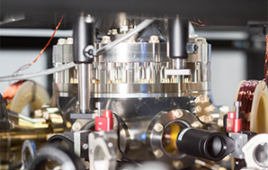
In IBM’s labs, tiny rivers of water are cooling computer chips that have circuits and components stacked on top of each other, a design that promises to advance
 |
Moore’s Law in the next decade and significantly reduce energy consumed by data centers. Researchers, in collaboration with the Fraunhofer Institute in Berlin, demonstrated a prototype that integrates the cooling system into the 3-D chips by piping water directly between each layer in the stack.
These so-called 3-D chip stacks — which take chips and memory devices that traditionally sit side-by-side on a silicon wafer and stack them together on top of one another — present one of the most promising approaches to enhancing chip performance beyond its predicted limits.
“As we package chips on top of each other to significantly speed a processor’s capability to process data, we have found that conventional coolers attached to the back of a chip don’t scale. In order to exploit the potential of high-performance 3-D chip stacking, we need interlayer cooling,” explains Thomas Brunschwiler, project leader at IBM’s Zurich Research Laboratory. “Until now, nobody has demonstrated viable solutions to this problem.”
3-D chip stacks would have an aggregated heat dissipation of close to 1 kilowatt — 10 times greater than the heat generated by a — with an area of four square centimeters and a thickness of about one millimeter. Moreover, each layer poses an additional barrier to heat removal.
Brunschwiler and his team piped water into cooling structures as thin as a human hair (50 microns) between the individual chip layers in order to remove heat efficiently at the source. Using the superior thermophysical qualities of water, scientists were able to demonstrate a cooling performance of up to 180 W/cm2 per layer for a stack with a typical footprint of 4 cm2.
“This truly constitutes a breakthrough. With classic backside cooling, the stacking of two or more high-power density logic layers would be impossible,” said Bruno Michel, manager of the chip cooling research efforts at the IBM Zurich Lab.
Technological specifications
In these experiments, scientists piped water through a 1x 1 cm test vehicle, consisting of a cooling layer between two dies or heat sources. The cooling layer measures only about 100 microns in height and is packed with 10,000 vertical interconnects per square centimeter.
The team overcame key technical challenges in designing a system that maximizes the water flow through the layers, yet hermetically seals the interconnects to prevent water from causing electrical shorts. The complexity of such a system resembles that of a human brain, wherein millions of nerves and neurons for signal transmissions are intermixed but do not interfere with tens of thousands of blood vessels for cooling and energy supply, all within the same volume.
The fabrication of the individual layers was accomplished with existing fabrication methods, except those needed to etch or drill the holes for signal transmission from one layer to the next. To insulate these “nerves,” scientists left a silicon wall around each interconnect (also called through silicon vias) and added a fine layer of silicon oxide to insulate the electrical interconnects from the water. The structures had to be fabricated to an accuracy of 10 microns, 10 times more accurate than for interconnects and metallizations in current chips.
To assemble the individual layers, Brunschwiler with colleagues from the Fraunhofer Institute developed a sophisticated thin-film soldering technique. Using this technique, scientists achieved the high-quality, precision and robustness needed to ensure excellent thermal contacts as well as electrical contacts without shorts. In the final setup, the assembled stack is placed in a silicon cooling container resembling a miniature basin. The water is pumped into the container from one side and flows between the individual chip layers before exiting at the other side.
Using simulations, scientists extrapolated the experimental results of their test vehicle to a 4-cm2 chip stack and achieved a cooling performance of 180 W/cm2.
In further research, Brunschwiler and his team are working to optimize cooling systems for even smaller chip dimensions and more interconnects. They also are investigating additional sophisticated structures for hotspot cooling.
Chip-cooling innovations
This most recent advancement is part of IBM’s ambitious research efforts focused on cooling technologies that allow the reuse of heat generated by data centers by capturing water at its hottest and piping it into the building’s water and heating systems. This announcement marks an important step toward that goal by succeeding in getting water to the hottest parts of the computer chip, where cooling is critical. The results were presented in a paper entitled “Forced convective interlayer cooling in vertically integrated packages” at the IEEE ITherm conference in Orlando, Florida, where it received a Best Paper award.