Research & Development World

  • R&D World Home
  • Topics
    • Aerospace
    • Automotive
    • Biotech
    • Careers
    • Chemistry
    • Environment
    • Energy
    • Life Science
    • Material Science
    • R&D Management
    • Physics
  • Technology
    • 3D Printing
    • A.I./Robotics
    • Software
    • Battery Technology
    • Controlled Environments
      • Cleanrooms
      • Graphene
      • Lasers
      • Regulations/Standards
      • Sensors
    • Imaging
    • Nanotechnology
    • Scientific Computing
      • Big Data
      • HPC/Supercomputing
      • Informatics
      • Security
    • Semiconductors
  • R&D Market Pulse
  • R&D 100
    • Call for Nominations: The 2025 R&D 100 Awards
    • R&D 100 Awards Event
    • R&D 100 Submissions
    • Winner Archive
    • Explore the 2024 R&D 100 award winners and finalists
  • Resources
    • Research Reports
    • Digital Issues
    • R&D Index
    • Subscribe
    • Video
    • Webinars
  • Global Funding Forecast
  • Top Labs
  • Advertise
  • SUBSCRIBE

Tunnel Junction, What’s Your Function?

By Yokohama National University | October 12, 2018

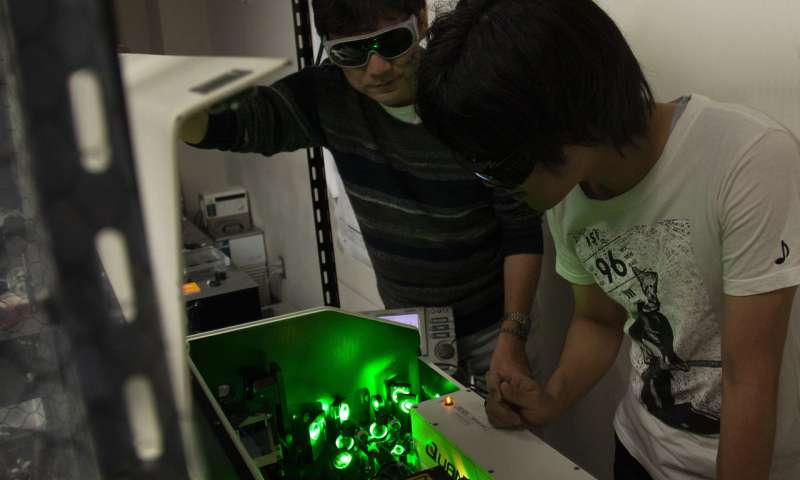
Prof. Jun Takeda (left) and Katsumasa Yoshioka (right). Image: Yokohama National University

Researchers from Japan have taken a step toward faster and more advanced electronics by developing a better way to measure and manipulate conductive materials through scanning tunneling microscopy.

The team published their results in July in Nano Letters, an American Chemical Society journal.

Scientists from the University of Tokyo, Yokohama National University, and the Central Research Laboratory of Hamamatsu Photonics contributed to this paper.

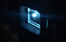
Scanning tunneling microscopy (STM) involves placing a conducting tip close to the surface of the conductive material to be imaged. A voltage is applied through the tip to the surface, creating a “tunnel junction” between the two through which electrons travel.

The shape and position of the tip, the voltage strength, and the conductivity and density of the material’s surface all come together to provide the scientist with a better understanding of the atomic structure of the material being imaged.

With that information, the scientist should be able to change the variables to manipulate the material itself.

Precise manipulation, however, has been a problem — until now.

The researchers designed a custom terahertz pulse cycle that quickly oscillates between near and far fields within the desired electrical current.

“The characterization and active control of near fields in a tunnel junction are essential for advancing elaborate manipulation of light-field-driven processes at the nanoscale,” says Jun Takeda, a professor in the department of physics in the Graduate School of Engineering at Yokohama National University.

“We demonstrated that desirable phase-controlled near fields can be produced in a tunnel junction via terahertz scanning tunneling microscopy with a phase shifter.”

According to Takeda, previous studies in this area assumed that the near and far fields were the same — spatially and temporally. His team examined the fields closely and not only identified that there was a difference between the two, but realized that the pulse of fast laser could prompt the needed phase shift of the terahertz pulse to switch the current to the near field.

“Our work holds enormous promise for advancing strong-field physics in nanoscale solid state systems, such as the phase change materials used for optical storage media in DVDs and Blu-ray, as well as next-generation ultrafast electronics and microscopies,” Takeda says.

Source: Yokohama National University

Related Articles Read More >

Illustration of ultracold atoms (gold) flowing frictionlessly along a laser boundary (green), representing the quantum phenomenon of edge states.
MIT physicists directly observe frictionless ‘edge state’ flow in ultracold atoms, offering a glimpse of super-efficient electronics
NTT Research scientist in cleanroom suit working on advanced photonic equipment
NTT Research bets light-based computing can tackles AI’s energy crisis
Scientists claim to generate world’s strongest terahertz radiation
SLAC fires up the world’s most powerful X-ray laser: LCLS-II ushers in a new era of science
rd newsletter
EXPAND YOUR KNOWLEDGE AND STAY CONNECTED
Get the latest info on technologies, trends, and strategies in Research & Development.
RD 25 Power Index

R&D World Digital Issues

Fall 2024 issue

Browse the most current issue of R&D World and back issues in an easy to use high quality format. Clip, share and download with the leading R&D magazine today.

Research & Development World
  • Subscribe to R&D World Magazine
  • Enews Sign Up
  • Contact Us
  • About Us
  • Drug Discovery & Development
  • Pharmaceutical Processing
  • Global Funding Forecast

Copyright © 2025 WTWH Media LLC. All Rights Reserved. The material on this site may not be reproduced, distributed, transmitted, cached or otherwise used, except with the prior written permission of WTWH Media
Privacy Policy | Advertising | About Us

Search R&D World

  • R&D World Home
  • Topics
    • Aerospace
    • Automotive
    • Biotech
    • Careers
    • Chemistry
    • Environment
    • Energy
    • Life Science
    • Material Science
    • R&D Management
    • Physics
  • Technology
    • 3D Printing
    • A.I./Robotics
    • Software
    • Battery Technology
    • Controlled Environments
      • Cleanrooms
      • Graphene
      • Lasers
      • Regulations/Standards
      • Sensors
    • Imaging
    • Nanotechnology
    • Scientific Computing
      • Big Data
      • HPC/Supercomputing
      • Informatics
      • Security
    • Semiconductors
  • R&D Market Pulse
  • R&D 100
    • Call for Nominations: The 2025 R&D 100 Awards
    • R&D 100 Awards Event
    • R&D 100 Submissions
    • Winner Archive
    • Explore the 2024 R&D 100 award winners and finalists
  • Resources
    • Research Reports
    • Digital Issues
    • R&D Index
    • Subscribe
    • Video
    • Webinars
  • Global Funding Forecast
  • Top Labs
  • Advertise
  • SUBSCRIBE