Researchers the world round are working to develop optical chips, where light can be controlled with nanostructures. These could be used for future circuits based on light (photons) instead of electron – that is photonics instead of electronics. But it has proved to be impossible to achieve perfect photonic nanostructures: they are inevitably a little bit imperfect.
Now, researchers at the Niels Bohr Institute in collaboration with DTU have discovered that imperfect nanostructures can offer entirely new functionalities. They have shown that imperfect optical chips can be used to produce ”nanolasers,” which is an ultimately compact and energy-efficient light source. The results are published in the scientific journal Nature Nanotechnology.
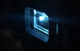
The researchers are working with extremely small photonic crystal membranes – the width of the membrane is 25 micrometer (1 micrometer is one thousandth of a millimeter), and the thickness is 340 nanometers (1 nanometer is one thousandth of a micrometer). The crystals are made of the semiconducting material gallium arsenide (GaAs). A pattern of holes are etched into the material at a regular distance of 380 nanometers. The holes have the function of acting as built-in mirrors that reflect the light and can thus be used to control the spread of the light in the optical chip. The researchers have therefore tried to achieve as perfect a regular structure of holes as possible to control the light in certain optical circuit.
But in practice it is impossible to avoid small irregularities during the manufacture of the optical chips and this can be a big problem, as it can result in the loss of light and therefore reduced functionality. Researchers at the Niels Bohr Institute have now turned the problem of imperfections into an advantage.
“It turns out that the imperfect optical chips are extremely well suited for capturing light. When the light is sent into the imperfect chip, it will hit the many small irregular holes, which reflect the light in random directions. Due to the frequent reflections, the light is spontaneously captured in the nanostructure and cannot escape. This allows the light to be amplified, resulting in surprisingly good conditions for creating highly efficient and compact lasers,” explains Peter Lodahl, professor and head of the Quantum Photonic research group at the Niels Bohr Institute at the University of Copenhagen.
 The researchers in Quantum Photonics at the Niels Bohr Institute, led by Professor Peter Lodahl and Associate Professor Søren Stobbe, designed the photonic crystal and carried out the experimental studies in the research group’s laboratories.
The light source is integrated into the photonic crystal itself and is comprised of a layer of artificial atoms that emit light (the basic component of light is photons). The photons are sent through the crystal, which is clear as glass and has a pattern of tiny holes. When a photon hits a hole it is reflected and channeled into the so-called waveguide, which is a ‘photon track’ that can be used to guide the photons through the photonic crystal. However, due to the imperfect holes the light will be thrown back and forth in the waveguide of the photonic crystal, intensifying it and turning it into laser light. The result is laser light on a nanometer scale and the researchers see great potential in this.
 “The fact that we can control the light and produce laser light on a nanometer scale can be used to create circuits based on photons instead of electrons, thus paving the way for optical quantum communication technology in the future. With built-in laser sources, we will be able to integrate optical components and it allows for the building of complex functionalities. Our ultimate dream is to build a “quantum Internet,” where the information is coded in individual photons,” explain Peter Lodahl and Søren Stobbe, who are excited about the results, which show that the unavoidable disorder in optical chip is not a limitation and can even be exploited under the right conditions.
Release Date: March 23, 2014
Source: Niels Bohr Institute