 Millimeter-sized crystals of high-quality graphene can be made in minutes instead of hours using a new scalable technique, Oxford University researchers have demonstrated.
In just 15 minutes the method can produce large graphene crystals around 2 to 3 millimeters in size that it would take up to 19 hours to produce using current chemical vapor deposition (CVD) techniques in which carbon in gas reacts with, for example, copper to form graphene.
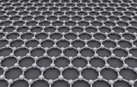
Graphene promises to be a “wonder material” for building new technologies because of its combination of strength, flexibility, electrical properties, and chemical resistance. But this promise will only be realized if it can be produced cost-effectively on a commercial scale.
The researchers took a thin film of silica deposited on a platinum foil which, when heated, reacts to create a layer of platinum silicide. This layer melts at a lower temperature than either platinum or silica creating a thin liquid layer that smooths out nanoscale “valleys” in the platinum so that carbon atoms in methane gas brushing the surface are more inclined to form large flakes of graphene.
A report of the research is published in the journal Nature Communications.
“Not only can we make millimeter-sized graphene flakes in minutes but this graphene is of a comparable quality to anything other methods are able to produce,” says Professor Nicole Grobert of Oxford University’s Department of Materials, who led the research. “Because it is allowed to grow naturally in single graphene crystals there are none of the grain boundaries that can adversely affect the mechanical and electrical properties of the material.”
Co-author Vitaliy Babenko, a DPhil student at Oxford University’s Department of Materials, says, “Using widely-available polycrystalline metals in this way can open up many possibilities for cost-reduction and larger-scale graphene production for applications where very high quality graphene is needed.”
Size-wise the new approach compares favorably with the common “Scotch tape method,” in which a piece of tape is used to peel graphene fragments off a chunk of graphite, which produces flakes of around 10 microns (0.01 millimeters). Using CVD with just platinum creates flakes of around 80 microns (0.08mm). But with the liquid layer of platinum silicide the researchers show that graphene crystals of 2-3 millimeters can be produced in minutes.
Out of all the techniques currently used to make different types of graphene CVD is the most promising for scaling up into a cost-effective industrial process. The Oxford team believe that their approach could also have benefits beyond speed and quality: with a thicker liquid layer to insulate it the graphene might not have to be removed from the substrate before it can be used — a costly and time-consuming additional step required with all other methods.
“This is a proof of principle study that shows that high-quality graphene, in the form of a single layer of carbon atoms, can be made to the size and timescale that someone looking to build technologies might want,” says Professor Grobert. “Of course a great deal more work is required before we get graphene technology, but we’re now on the cusp of seeing this material make the leap from the laboratory to a manufacturing setting, and we’re keen to work with industrial partners to make this happen.”
The researchers say that, in theory, it would be possible to further develop and scale up this technique to produce flakes of graphene in large wafer-sized sheets.
Release Date: June 15, 2015
Source: Oxford University


