Research & Development World

  • R&D World Home
  • Topics
    • Aerospace
    • Automotive
    • Biotech
    • Careers
    • Chemistry
    • Environment
    • Energy
    • Life Science
    • Material Science
    • R&D Management
    • Physics
  • Technology
    • 3D Printing
    • A.I./Robotics
    • Software
    • Battery Technology
    • Controlled Environments
      • Cleanrooms
      • Graphene
      • Lasers
      • Regulations/Standards
      • Sensors
    • Imaging
    • Nanotechnology
    • Scientific Computing
      • Big Data
      • HPC/Supercomputing
      • Informatics
      • Security
    • Semiconductors
  • R&D Market Pulse
  • R&D 100
    • Call for Nominations: The 2025 R&D 100 Awards
    • R&D 100 Awards Event
    • R&D 100 Submissions
    • Winner Archive
    • Explore the 2024 R&D 100 award winners and finalists
  • Resources
    • Research Reports
    • Digital Issues
    • R&D Index
    • Subscribe
    • Video
    • Webinars
  • Global Funding Forecast
  • Top Labs
  • Advertise
  • SUBSCRIBE

“Wonder” Material Revolutionizes Flexible Technology

By University of Warwick | February 15, 2017

Gadgets are set to become flexible, highly efficient and much smaller, following a breakthrough in measuring two-dimensional “wonder” materials by the University of Warwick.

Dr. Neil Wilson in the Department of Physics has developed a new technique to measure the electronic structures of stacks of two-dimensional materials — flat, atomically thin, highly conductive, and extremely strong materials — for the first time.

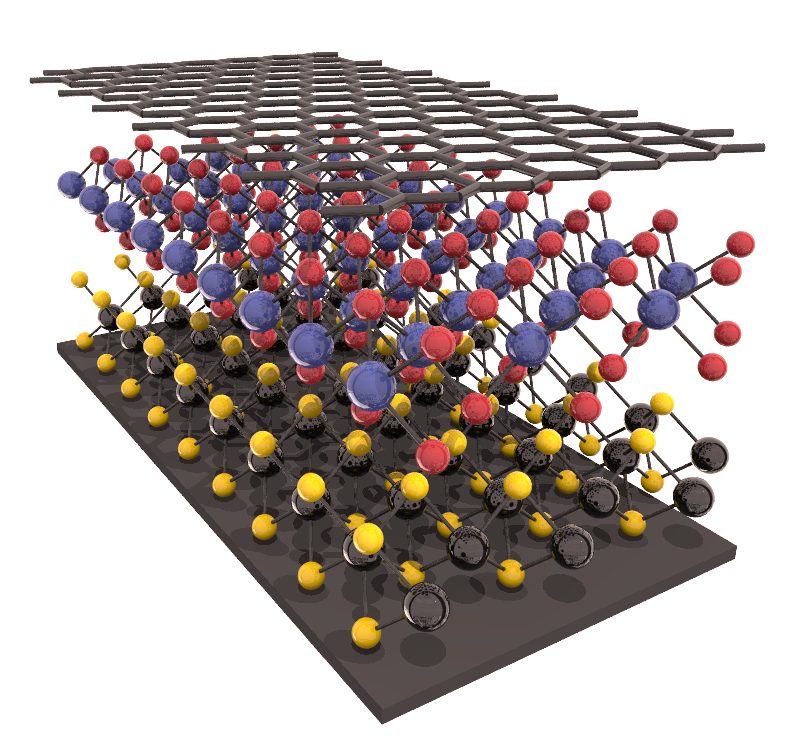
Multiple stacked layers of 2D materials — known as heterostructures — create highly efficient optoelectronic devices with ultrafast electrical charge, which can be used in nano-circuits, and are stronger than materials used in traditional circuits.

Various heterostructures have been created using different 2D materials — and stacking different combinations of 2D materials creates new materials with new properties.

Wilson’s technique measures the electronic properties of each layer in a stack, allowing researchers to establish the optimal structure for the fastest, most efficient transfer of electrical energy.

The technique uses the photoelectric effect to directly measure the momentum of electrons within each layer and shows how this changes when the layers are combined.

The ability to understand and quantify how 2D material heterostructures work — and to create optimal semiconductor structures – paves the way for the development of highly efficient nano-circuitry, and smaller, flexible, more wearable gadgets.

Solar power could also be revolutionized with heterostructures, as the atomically thin layers allow for strong absorption and efficient power conversion with a minimal amount of photovoltaic material.

Wilson comments on the work, “It is extremely exciting to be able to see, for the first time, how interactions between atomically thin layers change their electronic structure. This work also demonstrates the importance of an international approach to research; we would not have been able to achieve this outcome without our colleagues in the U.S.A. and Italy.”

Wilson worked formulated the technique in collaboration with colleagues in the theory groups at the University of Warwick and University of Cambridge, at the University of Washington in Seattle, and the Elettra Light Source, near Trieste in Italy.

Understanding how interactions between the atomic layers change their electronic structure required the help of computational models developed by Dr. Nick Hine, also from Warwick’s Department of Physics.

The paper, “Determination of band offsets, hybridization, and exciton binding in 2D semiconductor heterostructures,” is published in Science Advances.

Source: University of Warwick

Related Articles Read More >

Probiotics power a bioresorbable battery that can run from 4 to 100+ minutes
Korean engineers show off ultra-light prosthetic hand with single-motor thumb
2025 R&D layoffs tracker tops 92,000
Eli Lilly facility
9 R&D developments this week: Lilly builds major R&D center, Stratolaunch tests hypersonic craft, IBM chief urges AI R&D funding
rd newsletter
EXPAND YOUR KNOWLEDGE AND STAY CONNECTED
Get the latest info on technologies, trends, and strategies in Research & Development.
RD 25 Power Index

R&D World Digital Issues

Fall 2024 issue

Browse the most current issue of R&D World and back issues in an easy to use high quality format. Clip, share and download with the leading R&D magazine today.

Research & Development World
  • Subscribe to R&D World Magazine
  • Enews Sign Up
  • Contact Us
  • About Us
  • Drug Discovery & Development
  • Pharmaceutical Processing
  • Global Funding Forecast

Copyright © 2025 WTWH Media LLC. All Rights Reserved. The material on this site may not be reproduced, distributed, transmitted, cached or otherwise used, except with the prior written permission of WTWH Media
Privacy Policy | Advertising | About Us

Search R&D World

  • R&D World Home
  • Topics
    • Aerospace
    • Automotive
    • Biotech
    • Careers
    • Chemistry
    • Environment
    • Energy
    • Life Science
    • Material Science
    • R&D Management
    • Physics
  • Technology
    • 3D Printing
    • A.I./Robotics
    • Software
    • Battery Technology
    • Controlled Environments
      • Cleanrooms
      • Graphene
      • Lasers
      • Regulations/Standards
      • Sensors
    • Imaging
    • Nanotechnology
    • Scientific Computing
      • Big Data
      • HPC/Supercomputing
      • Informatics
      • Security
    • Semiconductors
  • R&D Market Pulse
  • R&D 100
    • Call for Nominations: The 2025 R&D 100 Awards
    • R&D 100 Awards Event
    • R&D 100 Submissions
    • Winner Archive
    • Explore the 2024 R&D 100 award winners and finalists
  • Resources
    • Research Reports
    • Digital Issues
    • R&D Index
    • Subscribe
    • Video
    • Webinars
  • Global Funding Forecast
  • Top Labs
  • Advertise
  • SUBSCRIBE