Caption: Researchers have developed a new material that could pave the way for flexible technology.
A new 2D ‘wonder’ material will help produce flexible, highly efficient and much smaller electronic devices.
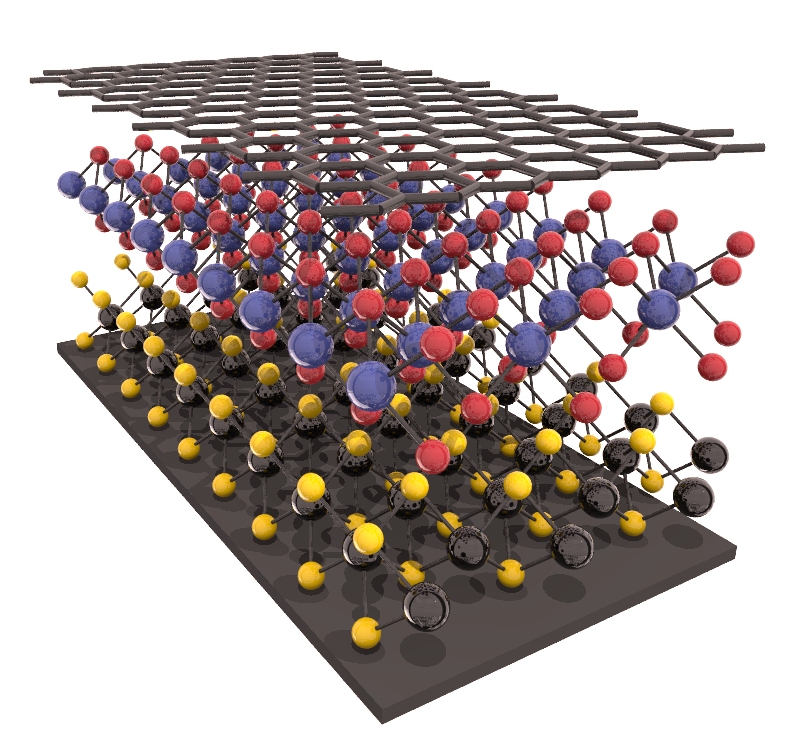
Researchers from the University of Warwick in England have developed a new technique to measure the electronic structures of stacks of flat, atomically thin, highly conductive, extremely strong 2D materials.
Multiple stacked layers of 2D materials—known as heterostructures—can create highly efficient optoelectronic devices with ultrafast electrical charge that can be used in nano-circuits and are stronger than materials used in traditional circuits.
Neil Wilson, Ph.D., professor in the Department of Physics, developed a technique that measures the electronic properties of each layer in a stack, allowing researchers to establish the optimal structure for the fastest, most efficient transfer of electrical energy.
“It is extremely exciting to be able to see, for the first time, how interactions between atomically thin layers change their electronic structure,” Wilson said in a statement. “This work also demonstrates the importance of an international approach to research; we would not have been able to achieve this outcome without our colleagues in the USA and Italy.”
According to the study, by combining monolayers of different two-dimensional semiconductors into heterostructures, researchers can create new phenomena and device possibilities. By understanding and exploiting these phenomena, researchers can determine the electronic structure and the properties of interlayer excitations.
The researchers were able to determine the key unknown parameters in MoSe2/WSe2 heterobilayers by using rational device design and submicrometer angle-resolved photoemission spectroscopy (μ-ARPES) in combination with photoluminescence.
They found that the bands in the K-point valleys are weakly hybridized with a valence band offset of 300 meV, implying type II band alignment.
Wilson’s technique uses the photoelectric effect to directly measure the momentum of electrons within each layer and show how this changes when the layers are combined.
The ability to understand and quantify how 2D material heterostructures work and to create optimal semiconductor structures, paves the way for the development of highly efficient nano-circuitry and smaller, flexible, more wearable gadgets.
The material could also help revolutionize solar power, as the atomically thin layers allow for strong absorption and efficient power conversion with a minimal amount of photovoltaic material.
Wilson formulated his technique in a collaboration with researchers at the University of Warwick, the University of Cambridge, the University of Washington in Seattle and the Elettra Light Source near Trieste in Italy.
The study was published in Sciences Advances.


