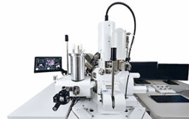
 ZEISS introduces its new integrated in situ workflow for ZEISS field emission scanning electron microscopes (FE-SEM). When researchers need to link material performance to microstructure, which is essential for developing novel materials in a highly efficient way, they can now extend their ZEISS FE-SEM with an in-situ solution for heating and tensile experiments. This allows them to observe materials like metals, alloys, polymers, plastics, composites and ceramics under heat and tension automatically while plotting stress-strain curves on the fly. They can control all system components from a single PC with a unified software environment that enables unattended automated materials testing for up to 24 hours. Core imaging facilities and materials research labs in academia, government and industry will equally benefit from this new solution.
Gaining deeper insights into material properties
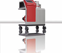
In situ materials testing in the SEM delivers precise measurement of the dynamic response of microstructures to mechanical load under defined temperature conditions. Thanks to the design of ZEISS Gemini electron optics, the integration of in situ hardware is very straightforward. Materials scientists can easily add information such as local chemical composition or crystallographic orientations using combined analytical techniques (for example, EDS and EBSD). All ZEISS FE-SEMs are plugged into the ZEISS ZEN core ecosystem, giving users access to ZEN Connect, ZEN Intellesis and ZEN’s analytical modules, for example.
“The ability to quantify material microstructure and bulk mechanical properties in a single automated, user-independent experimental environment provides researchers with the tools necessary to design next generation materials for the future low carbon economy. The in-situ lab is not only fully integrated, but service and application support are also included. What makes our solution unique is that users can define multiple regions of interest (ROIs) and therefore can be sure to never miss interesting areas of their sample,” said Dr. Michael Albiez, head of ZEISS Research Microscopy Solutions.
The solution is available for immediate upgrade on existing ZEISS GeminiSEM 360 and 460 and ZEISS Sigma 500 microscopes or can be purchased with new systems.
For more information, visit zeiss.com


Tell Us What You Think!