Research & Development World

  • R&D World Home
  • Topics
    • Aerospace
    • Automotive
    • Biotech
    • Careers
    • Chemistry
    • Environment
    • Energy
    • Life Science
    • Material Science
    • R&D Management
    • Physics
  • Technology
    • 3D Printing
    • A.I./Robotics
    • Software
    • Battery Technology
    • Controlled Environments
      • Cleanrooms
      • Graphene
      • Lasers
      • Regulations/Standards
      • Sensors
    • Imaging
    • Nanotechnology
    • Scientific Computing
      • Big Data
      • HPC/Supercomputing
      • Informatics
      • Security
    • Semiconductors
  • R&D Market Pulse
  • R&D 100
    • Call for Nominations: The 2025 R&D 100 Awards
    • R&D 100 Awards Event
    • R&D 100 Submissions
    • Winner Archive
    • Explore the 2024 R&D 100 award winners and finalists
  • Resources
    • Research Reports
    • Digital Issues
    • Educational Assets
    • R&D Index
    • Subscribe
    • Video
    • Webinars
  • Global Funding Forecast
  • Top Labs
  • Advertise
  • SUBSCRIBE

Diamonds, Quantum Information Processing on the Nano Scale

By The City University of New York | September 2, 2016

A City College of New York led-team headed by physicist Dr. Carlos Meriles has successfully demonstrated charge transport between Nitrogen-Vacancy color centers in diamond. The team developed a novel multi-color scanning microscopy technique to visualize the charge transport. The breakthrough experiment could potentially lead to room-temperature quantum information processing in diamond and optical data storage in three dimensions.

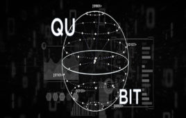
The nitrogen-vacancy (NV) center is an optically active defect in diamond comprising a nitrogen atom and an adjacent vacancy, replacing carbon atoms in the diamond lattice. This defect has electrons that are capable of storing quantum information. To utilize this special property for quantum computation, it is required to create a network of interacting NV centers. The research so far has focused on using photons emitted by the NV centers to create this interaction under a special low temperature environment.

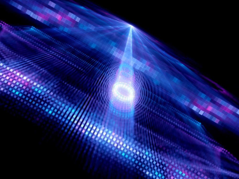
In a complementary approach the research team at City College in collaboration with researchers at the Australian National University (ANU) in Canberra are envisioning an electron-transport-based interaction that is realizable in ambient conditions. In one of the key experiments reported a focused green laser beam was used to remove the electrons from the NV centers, which later diffused radially in the diamond. A red laser scan was used to image NV centers that trapped these diffused charges as far as 30 microns. The team exploited the difference in luminescence intensities of the NV centers with and without the electron to create a map of the trapped carriers.

“These are very promising initial results” said lead author Dr. Harishankar Jayakumar, a postdoctoral fellow at the Meriles group. Other key contributors are CCNY team members Dr. Siddharth Dhomkar, and graduate student Jacob Henshaw, as well as Dr. Marcus Doherty and Prof. Neil Manson at ANU.

Related Articles Read More >

IBM’s second-generation, 156-qubit Quantum Heron processors offer reduced error rates, 16× better performance, and 25× faster speeds than 2022 systems. The Heron can run quantum circuits with up to 5,000 two-qubit gate operations using Qiskit—nearly double what IBM achieved in 2023.
Quantum computing edges closer to biotech reality in Moderna-IBM pact
Why IBM predicts quantum advantage within two years
Aardvark AI forecasts rival supercomputer simulations while using over 99.9% less compute
This week in AI research: Latest Insilico Medicine drug enters the clinic, a $0.55/M token model R1 rivals OpenAI’s $60 flagship, and more
rd newsletter
EXPAND YOUR KNOWLEDGE AND STAY CONNECTED
Get the latest info on technologies, trends, and strategies in Research & Development.
RD 25 Power Index

R&D World Digital Issues

Fall 2024 issue

Browse the most current issue of R&D World and back issues in an easy to use high quality format. Clip, share and download with the leading R&D magazine today.

Research & Development World
  • Subscribe to R&D World Magazine
  • Enews Sign Up
  • Contact Us
  • About Us
  • Drug Discovery & Development
  • Pharmaceutical Processing
  • Global Funding Forecast

Copyright © 2025 WTWH Media LLC. All Rights Reserved. The material on this site may not be reproduced, distributed, transmitted, cached or otherwise used, except with the prior written permission of WTWH Media
Privacy Policy | Advertising | About Us

Search R&D World

  • R&D World Home
  • Topics
    • Aerospace
    • Automotive
    • Biotech
    • Careers
    • Chemistry
    • Environment
    • Energy
    • Life Science
    • Material Science
    • R&D Management
    • Physics
  • Technology
    • 3D Printing
    • A.I./Robotics
    • Software
    • Battery Technology
    • Controlled Environments
      • Cleanrooms
      • Graphene
      • Lasers
      • Regulations/Standards
      • Sensors
    • Imaging
    • Nanotechnology
    • Scientific Computing
      • Big Data
      • HPC/Supercomputing
      • Informatics
      • Security
    • Semiconductors
  • R&D Market Pulse
  • R&D 100
    • Call for Nominations: The 2025 R&D 100 Awards
    • R&D 100 Awards Event
    • R&D 100 Submissions
    • Winner Archive
    • Explore the 2024 R&D 100 award winners and finalists
  • Resources
    • Research Reports
    • Digital Issues
    • Educational Assets
    • R&D Index
    • Subscribe
    • Video
    • Webinars
  • Global Funding Forecast
  • Top Labs
  • Advertise
  • SUBSCRIBE