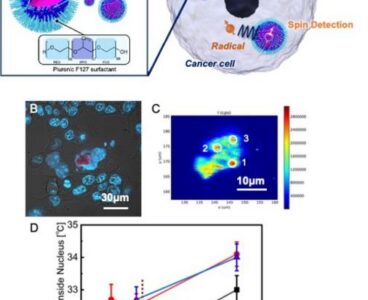
Researchers have developed molecular quantum nanosensors (MoQNs) designed to operate in the cytoplasm and nuclei of living cancer cells to map radical-generation processes and thermal dynamics that are linked to cancer-associated cellular physiology. The sensors use molecular-level uniformity to achieve a threefold enhancement in spectral resolution and superior thermometric specificity. The platform enables absolute temperature…
Overcoming the 100-nanometer barrier: New microbottle resonators scale up optical trapping
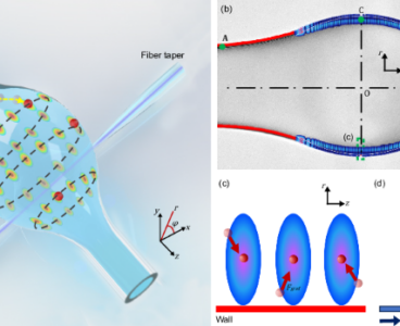
Near-field optical trapping allows for contact-free control of objects, including nanoparticles and living cells. This is traditionally done using whispering-gallery-mode and waveguide-based platforms that rely on evanescent fields that only penetrate about 100 nanometers into the surrounding medium. This shallow interaction restricts trapping efficiency and makes the system highly sensitive to perturbations, limiting the practical…
R&D 100 winner LLNL achieves 1,000x speed boost in 3D nanofabrication
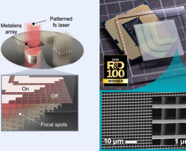
Researchers at Lawrence Livermore National Laboratory and Stanford University say they have built a two-photon lithography system that could push 3D nanofabrication toward manufacturing scale, boosting throughput by more than 1,000 times compared with commercial tools while maintaining minimum feature sizes of 113 nanometers. Two-photon lithography uses ultrafast laser pulses to harden material only at…
CEA-Leti achieves 400°C CMOS fabrication milestone for 3D chip stacking
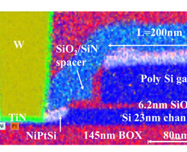
ChatGPT said: CEA-Leti announced it has built working 2.5-volt silicon-on-insulator CMOS chips at just 400°C. That is low enough to stack them atop finished circuitry without risking damage to the layers below, a hurdle that has long stalled progress toward denser, more efficient 3D chip designs. The French research institute, leading the EU’s FAMES pilot…
The 2025 R&D 100 Finalists are here

A total of 158 Finalists for the 2025 R&D 100 Awards have been announced by R&D World. Now in its 63rd year, this renowned global science and innovation competition drew entries from 13 countries/regions. This year’s esteemed judging panel featured 54 respected industry professionals from across the globe. The Finalists are listed below by category,…
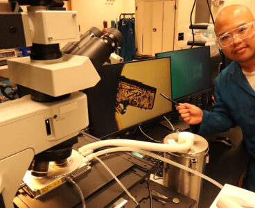
New nanotechnology method increases microalgae biofuel yield by 300%

Scientists from the University of Texas at El Paso demonstrated a new technique to improve the yield of biofuel from microalgae. Their study in ACS Applied Bio Materials centers on the microalga Chlorella vulgaris, which is commonly found in freshwater and can be used to produce biofuels. The researchers demonstrated that doses of zinc oxide…
New nanopore sensor paves the way for fast, accurate, low-cost DNA sequencing
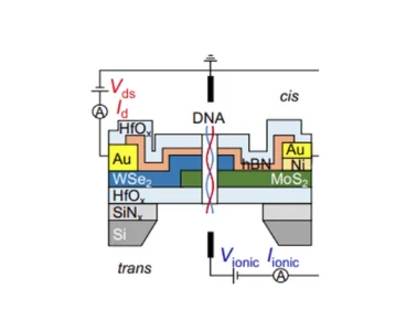
Researchers from the Grainger College of Engineering at the University of Illinois Urbana-Champaign have created a new nanopore sensor for single-biomolecule detection. Their findings were published in the journal PNAS. Nanopore sensors detect and analyze individual molecules by measuring ionic changes as the molecules pass through openings in the device. Nanopore sensors can be made…
Floating solar mats clean polluted water — and generate power
Most people bring a blanket to the beach to soak up the sun — this “blanket” soaks up pollution instead. Researchers at Ohio State University have created a solar-activated “nanomat” that floats on water like a beach mat, but instead of providing comfort, it goes to work cleaning up harmful contaminants. The lightweight, reusable material…
Nanodots enable fine-tuned light emission for sharper displays and faster quantum devices

Penn State and Université Paris-Saclay researchers report a new way to control light by embedding “nanodots” in ultra-thin, two-dimensional (2D) materials. The team says this precision could lead to higher-resolution screens and advances in quantum computing technologies. In a study published in ACS Photonics, the scientists demonstrated how these nanodots — tiny islands of a…
New photon-avalanching nanoparticles could enable next-generation optical computers
In the “Star Wars” universe, characters harness the power of light through iconic lightsabers. Here on Earth, researchers are tapping into a similarly transformative phenomenon, aiming to build technology that uses beams of light to perform ever-faster computing. A team co-led by Lawrence Berkeley National Laboratory (Berkeley Lab), Columbia University, and Universidad Autónoma de Madrid…
New “nose-computer interface” aims to upgrade Rover’s nose for better drug detection methods

When you take your dog for a walk, does he stop to sniff every tree trunk and patch of grass he sees, leaving you to wonder what smells so enticing? Scientists have also wondered, although not the trivial lawn fodder, what pups’ sensitive noses pick up to help detect drugs or disease. Lawrence Livermore National…
A smart ring with a tiny camera lets users point and click to control home devices

While smart home devices have expanded to include speakers, security systems, lights, and thermostats, their control has mostly been limited to a remote, an app, or voice commands. Users can interact with their phones or speak to the technology. Still, these methods are often less convenient than the simple switches they replace, significantly since devices…
Imec demonstrates long-term outdoor stability of perovskite solar modules
Imec, a partner in EnergyVille, in collaboration with the University of Cyprus, has reported significant progress in the development of perovskite solar modules, demonstrating long-term outdoor stability after two years of real-world testing. Mini-modules measuring 4 cm² retained 78% of their initial power conversion efficiency (PCE) after one year in outdoor conditions in Cyprus. This…
Stretchable batteries and body-conformable electronics poised to advance in 2025
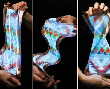
Stretchable, wearable gadgets took a significant stride in 2024, thanks to a flurry of breakthroughs that could make soft, body-conformable electronics and power sources a reality. Researchers worldwide have unveiled improvements in flexible, high-precision sensors and displays, while engineers in China revealed a self-healing, stretchable lithium-ion battery that could power next-generation wearables. Meanwhile, LG Display…
PPPL leading two CHIPS and Science Act projects

The U.S. Department of Energy (DOE) has awarded two grants to the Princeton Plasma Physics Laboratory (PPPL) as part of a significant effort to advance microelectronics and sensors. Each project will receive $3 million per year for four years, recognizing PPPL’s expertise in plasma processes, which are crucial for the continued development of semiconductor manufacturing…
Color-changing, power-free sensor could boost health monitoring and improve infrastructure safety
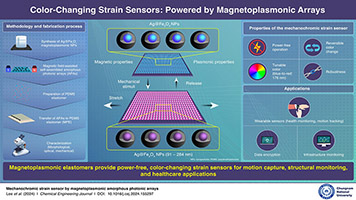
Researchers at Chungnam National University, Daejeon, South Korea, have developed a mechanochromic strain sensor that indicates mechanical stress through changing colors — without needing an external power source. The device, described in a study published on October 15, 2024, in the journal Chemical Engineering Journal, uses magnetic nanoparticles and elastic materials to detect stretching, bending,…
24 R&D trends that redefined 2024
In many respects, 2024 was a year of building upon the foundations laid by previous technological and scientific advances. While AI continued to evolve at a rapid clip, progress was in many ways more incremental than last year when GPT-4 redefined expectations for genAI. But AI continues to make definable improvements across a range of…
2024’s R&D Sustainability Innovator of the Year is looking for global collaborators
In the pursuit of sustainable energy, some inventors think big. Zhiyu (Jerry) Hu, Ph.D., thinks small — at the nanoscale. His work in thermoelectric devices is transforming how we understand and harvest energy, turning minute temperature differences into reliable power sources. For much of his life, Hu has found inspiration not just in fire but…
Oak Ridge National Lab leads R&D 100 Awards with 218 wins since 1979

An analysis of 45 years of R&D 100 Awards reveals a clear leader: Oak Ridge National Laboratory (ORNL), with more than two hundred winning products. National labs dominate the top ranks, demonstrating the staying power of consistent government investment in R&D. All of the top 10 organizations since 2010 are federally-backed entities. ORNL Frequently featured…
‘Slinky’ nanocrystals change color, potentially boosting microelectronics and cell research
A new class of nanoscale materials that act like microscopic mood rings, changing color with temperature, could help measure temperature at the tiniest scales, with potential applications in electronics, biology, and beyond. Published in Advanced Materials, this research from scientists at the University of California, Irvine involves a one-dimensional nanoscale material known as indium selenium…
Sandia Labs wants you to meet the “mother of all motion sensors”
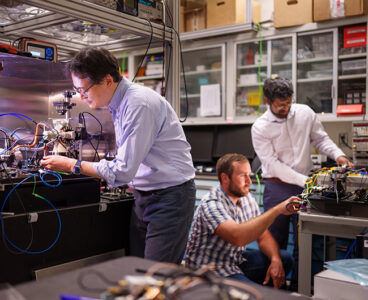
Peel apart a smartphone, fitness tracker, or virtual reality headset, and you’ll find a tiny motion sensor tracking its position and movement. Similar larger, more expensive versions exist that are about as big as a grapefruit and a thousand times more accurate. These devices aid GPS-assisted navigation in ships, airplanes, and other vehicles. Now imagine…
Explore the 2024 R&D 100 award winners and finalists

For six decades, the R&D 100 Awards have been a benchmark of achievement in science and technology, often referred to informally as “The Oscars of Innovation.” This year, we’re offering a new interactive experience, allowing you to explore the remarkable work of both winners and finalists across diverse fields. From advances in mechanical and material…
Imec sets record for lowest charge noise in silicon quantum dots on 300 mm CMOS platform
Imec, a research and innovation hub in nanoelectronics and digital technologies, has announced significant progress in the development of 300 mm silicon-based quantum dot spin qubit processing. The devices demonstrated an average charge noise of 0.6 µeV/√Hz at 1 Hz, the lowest values achieved on a 300 mm fab-compatible platform to date. These results are…
GIST researchers develop nanotechnology for quickly creating wafer-scale nanoparticle monolayers
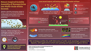
From the Gwangju Institute of Science and Technology (GIST) Controllable assembly of functional nanoparticles into uniform monolayers over large surfaces for industrial mass production has been a long-standing problem, especially when the particle size goes below 100 nm. A team of researchers from South Korea recently proposed a nature-inspired solution. Their new “one-shot” self-limiting assembly…
Pusan National University researchers boost signal amplification in perovskite nanosheets
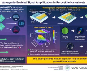
Perovskite nanosheets show distinctive characteristics with significant applications in science and technology. In a recent study, researchers from Korea and the U.K. achieved enhanced signal amplification in CsPbBr3 perovskite nanosheets with a unique waveguide pattern, which enhanced both gain and thermal stability. These advancements carry wide-ranging implications for laser, sensor, and solar cell applications and…