 Nanoengineering deals with structures at the nanoscale — between one and 100 nanometers. A nanometer (nm) is one billionth of a meter, and the distance between individual atoms in a solid is between 0.1 nm and 0.4 nm. The nanoscale is therefore about as small as materials can get, without becoming individual atoms. Nanotechnology and nanoengineering are essentially the same thing, but nanotechnology tends to be used more at the fundamental pure science stage, while nanoengineering is more about applications of the technology. Nanoengineering includes nanofabrication, nanomanufacturing, and measurement of nanoscale structures.
Scanning electron microscopes (SEM) and scanning tunneling microscopes (STM) can be used both to image and manipulate materials at the nanoscale. Electron microscopes have a similar principle to an optical microscope but use an electron beam rather than visible light. Due to the much shorter wavelength of an electron beam, they have a resolution better than one nanometer. A scanning tunneling microscope can be used to image surfaces at the nanoscale. It can also be used to move individual atoms. A very sharp tip is placed over an object within a vacuum, and moved in tiny increments over the surface using piezoelectric actuation. When the tip is close enough to surface, electrons tunnel through the vacuum in a process known as quantum tunneling. The resulting current provides sensing of the surface with a resolution of just 0.01 nm.
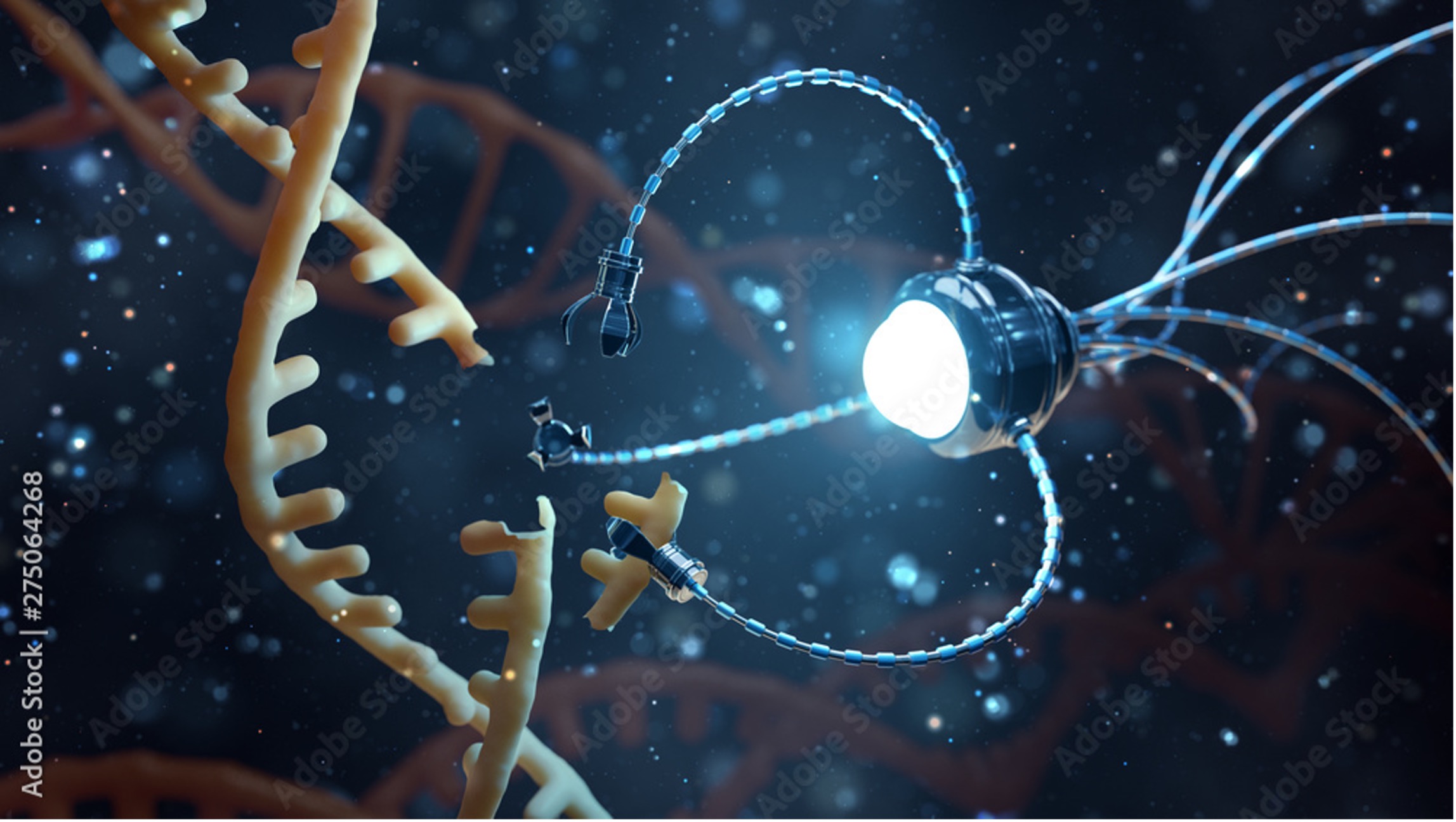
Nanomanufacturing produces nanoscale materials, structures and devices, using scalable, high-yield processes. Although one-day it may be possible to create microbe sized robots with nanoscale mechanical parts, todays nanomanufacturing generally involves the creation of simple repeating structures at the nanoscale. Nanoscale structures include active materials for electrodes used in batteries and fuel cells, and many semiconductor devices such as computer chips. Bulk materials include powders, graphene and carbon nanotubes.
Perhaps the most established form of nanomanufacturing is nanofabrication, which creates precisely defined structures at the nanoscale. Many of the methods used have been developed by the semiconductor industry, which uses a sequential process of thin film material deposition, patterning and etching, to produce electronic circuits. For example, integrated circuits are created with transistors formed from the intersections of conducting metal fins arranged in a grid pattern. Although originally these processes were used to produce much larger circuits, over the last twenty years they have moved into the nanoscale. In the most advanced ‘5 nm process’ computer chips, the grids have metal fins spaced at a pitch of approximately 20 nm.
The first stage of the semiconductor fabrication process, thin film material deposition, involves depositing layers of metallic material on a semiconductor substrate. Deposition can be carried out using vacuum evaporation, sputter deposition or chemical vapor deposition. This layered material is then patterned, selectively removing the upper layer to form the electronic circuit. Patterning methods include photolithography, electron-beam lithography and nano-imprint lithography. Lithography uses a mask to preserve material while the material below the gaps in the mask are vaporized by a laser or electron-beam — much like a stencil.
Subsequent layers may then be removed by etching, with processes classified as wet or dry etching. Chemical wet etching uses reactive liquids such acids, bases and solvents. Dry etching uses reactive gases in processes including reactive ion etching and conductively coupled plasma etching. Nanofabrication must be performed in a clean room. In addition to the major semiconductor production processes described above, newer nanofabrication processes include quantum dots, nanowires and self assembly.
Nanoscale materials such as nanoparticles and nanostructured materials are produced using bulk processes which often do not require the type of direct control at the nanoscale seen in nanofabrication. These materials can be produced through a top-down process of breaking up large pieces of material into successively smaller pieces, or by a bottom-up process of assembling atoms or molecules into larger nanostructures. Nanostructured materials tend to have extremely large surface areas, causing them to exhibit properties such as high electrical and thermal conductivity, capacitance, and ion storage capacity. This means they have many applications in energy storage — enhancing the performance of batteries, supercapacitors, thermal energy storage, and hydrogen storage. There is currently particular interest in their ability to enhance the energy storage of anodes and cathodes in lithium-ion batteries.


Tell Us What You Think!