Researchers at Lawrence Livermore National Laboratory and Stanford University say they have built a two-photon lithography system that could push 3D nanofabrication toward manufacturing scale, boosting throughput by more than 1,000 times compared with commercial tools while maintaining minimum feature sizes of 113 nanometers.
Two-photon lithography uses ultrafast laser pulses to harden material only at the laser’s tight focal point, letting engineers “write” complex 3D structures with very fine detail. The technique is valued for resolution, but it has been slow and confined to small fields of view because most systems rely on microscope objectives. Printing anything larger typically requires stitching together thousands of tiny tiles, a workflow that takes time and can introduce alignment errors.
From a single focus to 120,000 spots
The new platform, described Dec. 17 in Nature, replaces the microscope objective with tiled arrays of metalenses, ultrathin optical elements engineered to shape light. Instead of scanning a single focus across a surface, the metalens array splits a femtosecond laser into more than 120,000 coordinated focal spots, allowing the system to write in parallel across centimeter-scale areas.
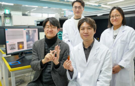
“It means two-photon lithography finally has the potential for industry adoption,” said Songyun Gu, an LLNL postdoctoral researcher and first author on the paper. Gu said wafer-scale nanomanufacturing could allow nanomaterials and microdevices to be produced more like computer chips, where complexity can be replicated at scale.
A second component, a spatial light modulator, lets the team adjust the intensity of each focal spot in real time. That capability helps equalize beam intensity, but it also enables more flexible patterning than simple repeating arrays. The system can switch individual beams on or off and tune linewidths with grayscale control, allowing fabrication of non-periodic and stochastic structures as well as regular patterns.
Achieving breakthrough speeds for industrial applications
LLNL principal investigator Xiaoxing Xia said the team was surprised by how quickly the concept translated into larger-area printing. “To see a print being done accurately at speed hundreds to thousands of times faster than our commercial printer, we realized a breakthrough has happened,” Xia said.
The researchers are exploring applications that include 3D-printed fusion fuel capsules, trapped-ion quantum computing chips, flexible terahertz devices and micro-particle manufacturing at rates of tens of millions per day. The platform, called MetaLitho3D, received a 2025 R&D 100 Award.
Looking ahead, the team said higher-power lasers, larger metalens wafers and faster modulators could further increase speed and enable more complex devices, as the approach moves from demonstration toward broader adoption.